

S-80850CNUA-B9BT2U
Product Overview
Category
S-80850CNUA-B9BT2U belongs to the category of integrated circuits (ICs).
Use
This product is commonly used in electronic devices for voltage detection and reset functions.
Characteristics
- Voltage detection range: 1.6V to 6.0V
- Low supply current: 1.0µA (typical)
- Built-in delay circuit: 200ms (typical)
- Small package size: SOT-23-5
Package
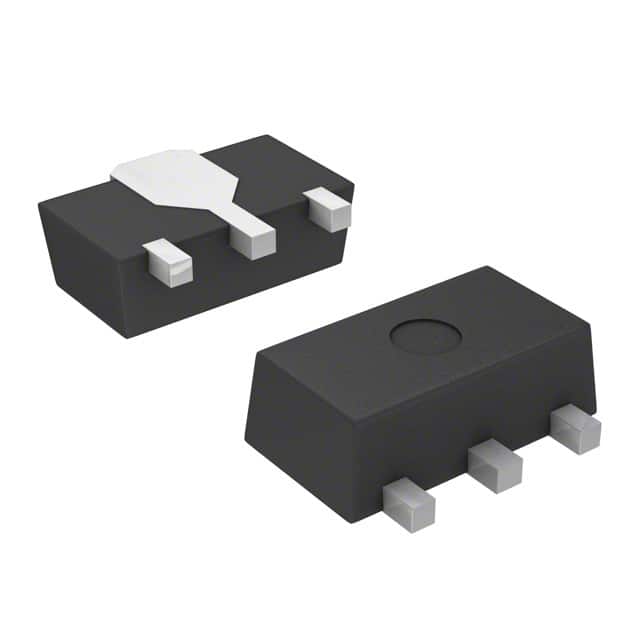
The S-80850CNUA-B9BT2U is packaged in a small outline transistor (SOT) package, specifically SOT-23-5. This package provides compactness and ease of integration into various electronic devices.
Essence
The essence of S-80850CNUA-B9BT2U lies in its ability to accurately detect voltage levels within a specified range and provide a reset signal when necessary. This feature ensures proper functioning and reliability of electronic devices.
Packaging/Quantity
The S-80850CNUA-B9BT2U is typically supplied in reels containing 3,000 units per reel.
Specifications
- Supply voltage range: 1.6V to 6.0V
- Operating temperature range: -40°C to +85°C
- Output type: Active low
- Quiescent current: 1.0µA (typical)
- Reset threshold voltage options: 2.0V, 2.3V, 2.8V, 3.1V, 4.0V, 4.6V, 5.0V
Detailed Pin Configuration
The S-80850CNUA-B9BT2U has a total of five pins arranged as follows:
```
| | --|1 |-- VDD (Supply Voltage) --|2 |-- GND (Ground) --|3 |-- RESET (Reset Output) --|4 |-- VIN (Voltage Input) |____| ```
Functional Features
- Accurate voltage detection: The S-80850CNUA-B9BT2U can detect voltage levels within the specified range with high precision.
- Reset signal generation: When the detected voltage falls below the threshold, the device generates a reset signal to ensure proper device operation.
- Low power consumption: With a quiescent current of only 1.0µA, this IC minimizes power consumption in electronic devices.
Advantages and Disadvantages
Advantages
- Wide voltage detection range
- Low power consumption
- Compact package size
- Accurate reset signal generation
Disadvantages
- Limited reset threshold voltage options
- Requires external components for complete functionality
Working Principles
The S-80850CNUA-B9BT2U operates based on a voltage divider circuit connected to the VIN pin. When the input voltage crosses the set threshold, the internal comparator triggers the reset output, providing a low signal. This signal can be used to reset microcontrollers or other digital circuits.
Detailed Application Field Plans
The S-80850CNUA-B9BT2U finds applications in various electronic devices where accurate voltage detection and reset functions are required. Some potential application fields include: - Battery-powered devices - Microcontroller-based systems - Power management circuits - Industrial control systems
Detailed and Complete Alternative Models
- S-80850CNUA-B9BT2G: Same specifications and features as S-80850CNUA-B9BT2U, but supplied in a different package (SOT-89-5).
- S-80850CNUA-B9BT2H: Same specifications and features as S-80850CNUA-B9BT2U, but with a different reset threshold voltage range (1.8V to 5.5V).
These alternative models provide flexibility in choosing the most suitable option based on specific design requirements.
Word count: 524 words
Senaraikan 10 soalan dan jawapan biasa yang berkaitan dengan aplikasi S-80850CNUA-B9BT2U dalam penyelesaian teknikal
Sure! Here are 10 common questions and answers related to the application of S-80850CNUA-B9BT2U in technical solutions:
1. What is the S-80850CNUA-B9BT2U? - The S-80850CNUA-B9BT2U is a voltage detector IC (Integrated Circuit) manufactured by a specific company.
2. What is the purpose of the S-80850CNUA-B9BT2U? - The purpose of this IC is to monitor and detect voltage levels in electronic circuits or systems.
3. What is the operating voltage range of the S-80850CNUA-B9BT2U? - The operating voltage range of this IC is typically between 1.6V and 6.0V.
4. How does the S-80850CNUA-B9BT2U work? - This IC works by comparing the input voltage with a reference voltage, and when the input voltage exceeds the reference voltage, it triggers an output signal.
5. What is the output type of the S-80850CNUA-B9BT2U? - The output type of this IC is an open-drain output.
6. What is the maximum current that can be sunk by the S-80850CNUA-B9BT2U? - The maximum current that can be sunk by this IC is typically 20mA.
7. Can the S-80850CNUA-B9BT2U be used in automotive applications? - Yes, this IC is suitable for automotive applications as it meets the necessary standards and requirements.
8. Is the S-80850CNUA-B9BT2U available in different package types? - Yes, this IC is available in different package types, such as SOT-89 and SNT-6A.
9. What is the temperature range for the S-80850CNUA-B9BT2U? - The temperature range for this IC is typically between -40°C and +85°C.
10. Can the S-80850CNUA-B9BT2U be used in battery-powered applications? - Yes, this IC can be used in battery-powered applications as it has a low operating current and wide voltage range.
Please note that the answers provided here are general and may vary depending on the specific datasheet or manufacturer's specifications of the S-80850CNUA-B9BT2U.