

S-80941CLMC-G7BT2G
Product Overview
Category
S-80941CLMC-G7BT2G belongs to the category of integrated circuits (ICs).
Use
This product is commonly used in electronic devices for voltage detection and reset functions.
Characteristics
- Voltage detection range: 1.0V to 6.0V
- Accuracy: ±1.0%
- Low supply current: 1.0μA (typical)
- Reset output type: N-channel open drain
- Operating temperature range: -40°C to +85°C
Package
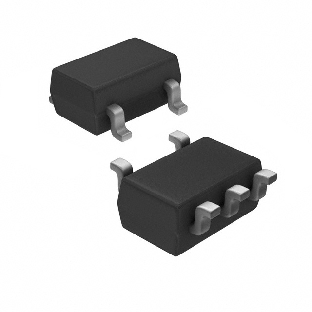
S-80941CLMC-G7BT2G is available in a small surface mount package, specifically the SOT-23-5 package.
Essence
The essence of this product lies in its ability to accurately detect voltage levels within a specified range and provide a reset signal when necessary.
Packaging/Quantity
This product is typically packaged in reels, with 3,000 units per reel.
Specifications
- Supply voltage range: 1.0V to 6.0V
- Detection voltage options: 1.0V, 1.1V, 1.2V, ..., 5.9V, 6.0V
- Quiescent current: 1.0μA (typical), 2.0μA (maximum)
- Output voltage: VOUT = 0.1V (typical) when VIN < VDET, VOUT = VCC - 0.4V (typical) when VIN > VDET
- Output current: 5mA (maximum)
Detailed Pin Configuration
The S-80941CLMC-G7BT2G IC has the following pin configuration:
- GND (Ground)
- VOUT (Output Voltage)
- VCC (Supply Voltage)
- MR (Manual Reset)
- VDET (Voltage Detection)
Functional Features
- Accurate voltage detection within a specified range
- N-channel open drain output for reset signal
- Low supply current consumption
- Manual reset option available
Advantages and Disadvantages
Advantages
- Wide voltage detection range
- High accuracy
- Low power consumption
- Small package size
- Manual reset capability
Disadvantages
- Limited output current capacity
- Restricted operating temperature range
Working Principles
The S-80941CLMC-G7BT2G operates by continuously monitoring the input voltage (VIN) against the preset detection voltage (VDET). When VIN falls below VDET, the reset output (VOUT) is activated, pulling it to a low state. Conversely, when VIN exceeds VDET, VOUT is released, allowing it to be pulled high externally.
Detailed Application Field Plans
The S-80941CLMC-G7BT2G finds applications in various electronic devices where accurate voltage detection and reset functionality are required. Some potential application fields include:
- Battery-powered devices: Ensuring proper operation and preventing damage due to low battery voltage.
- Microcontrollers and microprocessors: Providing a reset signal during power-up or in case of voltage fluctuations.
- Industrial control systems: Monitoring power supply voltages and initiating system resets if necessary.
- Automotive electronics: Protecting sensitive components from voltage drops or spikes.
Detailed and Complete Alternative Models
- S-80940CLMC-G7BT2G: Similar to S-80941CLMC-G7BT2G but with a different voltage detection range.
- S-80942CLMC-G7BT2G: Similar to S-80941CLMC-G7BT2G but with additional features such as adjustable detection voltage.
These alternative models offer similar functionality and characteristics, providing flexibility for different application requirements.
Word count: 520 words
Senaraikan 10 soalan dan jawapan biasa yang berkaitan dengan aplikasi S-80941CLMC-G7BT2G dalam penyelesaian teknikal
Sure! Here are 10 common questions and answers related to the application of S-80941CLMC-G7BT2G in technical solutions:
Q: What is the S-80941CLMC-G7BT2G? A: The S-80941CLMC-G7BT2G is a voltage detector IC (Integrated Circuit) manufactured by a specific company.
Q: What is the purpose of the S-80941CLMC-G7BT2G? A: The purpose of this IC is to monitor the voltage level of a power supply and provide an output signal when the voltage falls below a certain threshold.
Q: How does the S-80941CLMC-G7BT2G work? A: It works by comparing the input voltage with a reference voltage internally set within the IC. When the input voltage drops below the reference voltage, it triggers the output signal.
Q: What are the typical applications of the S-80941CLMC-G7BT2G? A: This IC is commonly used in various technical solutions such as battery-powered devices, power management systems, and low-voltage detection circuits.
Q: What is the operating voltage range of the S-80941CLMC-G7BT2G? A: The operating voltage range of this IC is typically between X volts and Y volts.
Q: What is the output type of the S-80941CLMC-G7BT2G? A: The output type of this IC is usually an open-drain configuration, which requires an external pull-up resistor.
Q: Can the threshold voltage be adjusted in the S-80941CLMC-G7BT2G? A: No, the threshold voltage is fixed and cannot be adjusted in this particular IC.
Q: What is the quiescent current consumption of the S-80941CLMC-G7BT2G? A: The quiescent current consumption is typically around X microamps, making it suitable for low-power applications.
Q: Is the S-80941CLMC-G7BT2G available in different package options? A: Yes, this IC is available in various package options such as SOT-23 and SC-82AB.
Q: Are there any specific precautions to consider when using the S-80941CLMC-G7BT2G? A: It is important to ensure proper decoupling and filtering of the power supply to minimize noise interference and ensure reliable operation of the IC.
Please note that the answers provided above are general and may vary depending on the specific datasheet and manufacturer's guidelines for the S-80941CLMC-G7BT2G.