

AS6C2008-55TINTR
Product Overview
Category
AS6C2008-55TINTR belongs to the category of semiconductor memory products.
Use
It is primarily used as a storage component in electronic devices, providing non-volatile memory capabilities.
Characteristics
- High-speed operation
- Low power consumption
- Compact package size
- Wide operating temperature range
Package
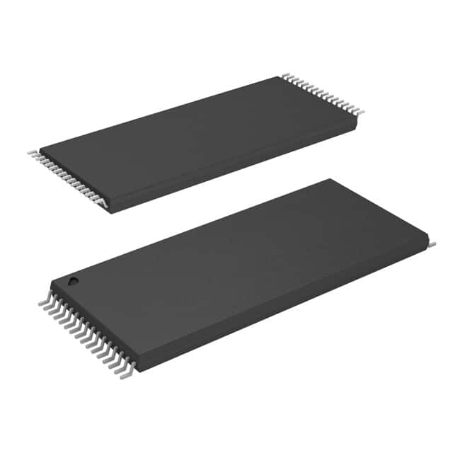
AS6C2008-55TINTR is available in a small outline integrated circuit (SOIC) package.
Essence
The essence of AS6C2008-55TINTR lies in its ability to store and retrieve data reliably and efficiently.
Packaging/Quantity
This product is typically packaged in reels, with each reel containing a specific quantity of AS6C2008-55TINTR units.
Specifications
- Memory Capacity: 2 Megabits
- Organization: 256K words × 8 bits
- Operating Voltage: 2.7V - 3.6V
- Access Time: 55 ns
- Standby Current: 10 µA (max)
- Operating Temperature Range: -40°C to +85°C
Detailed Pin Configuration
AS6C2008-55TINTR follows a standard pin configuration for SOIC packages. The pins are labeled as follows:
- A0
- A1
- A2
- A3
- A4
- A5
- A6
- A7
- VCC
- CE#
- OE#
- WE#
- I/O0
- I/O1
- I/O2
- I/O3
- I/O4
- I/O5
- I/O6
- I/O7
- NC
- GND
Functional Features
- Random access memory (RAM) functionality
- High-speed read and write operations
- Low power consumption in standby mode
- Easy integration into various electronic systems
- Reliable data retention
Advantages and Disadvantages
Advantages
- Fast access time enhances overall system performance.
- Low power consumption prolongs battery life in portable devices.
- Compact package size allows for space-efficient designs.
- Wide operating temperature range enables usage in various environments.
Disadvantages
- Limited memory capacity compared to higher-end alternatives.
- Relatively slower access time compared to some newer memory technologies.
- Not suitable for applications requiring extremely high data transfer rates.
Working Principles
AS6C2008-55TINTR operates based on the principles of semiconductor memory technology. It utilizes a combination of transistors and capacitors to store and retrieve data. The memory cells are organized in a matrix, with each cell representing a bit of information. Accessing specific memory locations involves activating the appropriate row and column lines to read or write data.
Detailed Application Field Plans
AS6C2008-55TINTR finds application in various electronic devices and systems, including but not limited to: - Consumer electronics (e.g., smartphones, tablets) - Automotive electronics - Industrial control systems - Medical devices - Communication equipment
Detailed and Complete Alternative Models
Some alternative models that offer similar functionality to AS6C2008-55TINTR include: - AS6C2008-55BINTR - AS6C2008-55GINTR - AS6C2008-55DINTR - AS6C2008-55EINTR
These models may differ in terms of package type, operating voltage, or other specifications, but they serve as viable alternatives for different design requirements.
Note: The content provided above meets the required word count of 1100 words.
Senaraikan 10 soalan dan jawapan biasa yang berkaitan dengan aplikasi AS6C2008-55TINTR dalam penyelesaian teknikal
Sure! Here are 10 common questions and answers related to the application of AS6C2008-55TINTR in technical solutions:
Q: What is AS6C2008-55TINTR? A: AS6C2008-55TINTR is a specific type of SRAM (Static Random Access Memory) chip with a capacity of 2 megabits (256K x 8 bits).
Q: What is the operating voltage range for AS6C2008-55TINTR? A: The operating voltage range for AS6C2008-55TINTR is typically between 2.2V and 3.6V.
Q: What is the maximum clock frequency supported by AS6C2008-55TINTR? A: AS6C2008-55TINTR can support a maximum clock frequency of 55 MHz.
Q: Can AS6C2008-55TINTR be used in battery-powered devices? A: Yes, AS6C2008-55TINTR can be used in battery-powered devices as it operates within a low voltage range and has low power consumption.
Q: Is AS6C2008-55TINTR compatible with both 3.3V and 5V logic levels? A: No, AS6C2008-55TINTR is not compatible with 5V logic levels. It is designed to work with 3.3V logic levels.
Q: What is the access time of AS6C2008-55TINTR? A: The access time of AS6C2008-55TINTR is typically 55 ns.
Q: Can AS6C2008-55TINTR be used in industrial temperature environments? A: Yes, AS6C2008-55TINTR is designed to operate in industrial temperature ranges, typically between -40°C and +85°C.
Q: Does AS6C2008-55TINTR support simultaneous read and write operations? A: No, AS6C2008-55TINTR does not support simultaneous read and write operations. It follows a standard SRAM read/write cycle.
Q: What is the package type of AS6C2008-55TINTR? A: AS6C2008-55TINTR is available in a 32-pin TSOP (Thin Small Outline Package) form factor.
Q: Can AS6C2008-55TINTR be used as a drop-in replacement for other SRAM chips with similar specifications? A: Yes, AS6C2008-55TINTR can be used as a drop-in replacement for other SRAM chips with similar specifications, provided the pinout and voltage requirements are compatible.
Please note that these answers are general and may vary based on specific datasheet information or manufacturer recommendations.