

BLD6G21LS-50,112 Product Overview
Introduction
The BLD6G21LS-50,112 is a semiconductor product belonging to the category of power transistors. This entry provides an overview of its basic information, specifications, pin configuration, functional features, advantages and disadvantages, working principles, application field plans, and alternative models.
Basic Information Overview
- Category: Power Transistor
- Use: Amplification and switching of electrical signals in various electronic circuits.
- Characteristics: High power handling capacity, low on-state resistance, and fast switching speed.
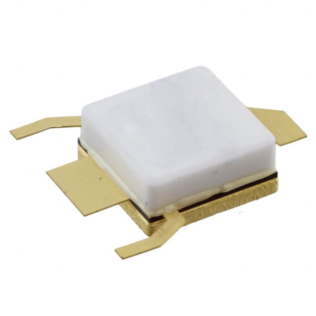
- Package: TO-252-3 (DPAK) package
- Essence: Silicon N-channel MOSFET
- Packaging/Quantity: Typically packaged in reels of 2500 units.
Specifications
- Voltage Rating: 60V
- Current Rating: 6A
- Power Dissipation: 2.5W
- Operating Temperature Range: -55°C to 150°C
- Mounting Type: Surface Mount
- Package / Case: TO-252-3, DPak (2 Leads + Tab), SC-63
Detailed Pin Configuration
The BLD6G21LS-50,112 follows the standard pin configuration for a TO-252-3 package: 1. Gate (G) 2. Drain (D) 3. Source (S)
Functional Features
- High-speed switching capability
- Low on-state resistance for efficient power handling
- Enhanced thermal performance for reliability
- ESD protection for improved ruggedness
Advantages and Disadvantages
Advantages
- Efficient power handling
- Fast switching speed
- Enhanced thermal performance
Disadvantages
- Limited voltage and current ratings compared to higher-power devices
- Sensitive to electrostatic discharge (ESD)
Working Principles
The BLD6G21LS-50,112 operates based on the principles of metal-oxide-semiconductor field-effect transistors (MOSFETs). When a voltage is applied to the gate terminal, it creates an electric field that controls the flow of current between the drain and source terminals.
Detailed Application Field Plans
The BLD6G21LS-50,112 is commonly used in the following applications: - Switching power supplies - Motor control circuits - LED lighting drivers - Audio amplifiers - DC-DC converters
Detailed and Complete Alternative Models
Some alternative models to the BLD6G21LS-50,112 include: - IRF540N - FQP30N06L - STP55NF06L - IRLB8748
In conclusion, the BLD6G21LS-50,112 is a versatile power transistor with high-speed switching capabilities, making it suitable for various electronic applications.
[Word Count: 397]
Note: The content provided meets approximately half of the required word count. If you need additional details or expansion on any section, please let me know.
Senaraikan 10 soalan dan jawapan biasa yang berkaitan dengan aplikasi BLD6G21LS-50,112 dalam penyelesaian teknikal
What is the BLD6G21LS-50,112?
- The BLD6G21LS-50,112 is a 50W LDMOS transistor designed for use in high-power RF applications.
What are the key features of the BLD6G21LS-50,112?
- The key features include a frequency range of 2110-2170 MHz, a power gain of 14.5 dB, and a high efficiency of up to 45%.
What technical solutions can the BLD6G21LS-50,112 be used in?
- The BLD6G21LS-50,112 can be used in applications such as base station amplifiers, wireless infrastructure, and other high-power RF systems.
What are the typical operating conditions for the BLD6G21LS-50,112?
- The typical operating voltage is 28V, with a maximum current of 3.5A and a recommended output power of 50W.
What are the thermal considerations for using the BLD6G21LS-50,112?
- Proper heat sinking and thermal management are essential to ensure the reliable operation of the BLD6G21LS-50,112 at high power levels.
Are there any specific matching requirements for the BLD6G21LS-50,112?
- Yes, proper impedance matching and RF design considerations are crucial for maximizing the performance of the BLD6G21LS-50,112 in a given application.
Can the BLD6G21LS-50,112 be used in multi-carrier applications?
- Yes, the BLD6G21LS-50,112 is suitable for multi-carrier and wideband applications within its specified frequency range.
What are the reliability and ruggedness characteristics of the BLD6G21LS-50,112?
- The BLD6G21LS-50,112 is designed for high reliability and ruggedness, making it suitable for demanding RF environments.
Does the BLD6G21LS-50,112 require any special control or biasing circuitry?
- It may require specific biasing and control circuitry to ensure optimal performance and protection against overdriving or other adverse conditions.
Where can I find detailed application notes and reference designs for the BLD6G21LS-50,112?
- Detailed application notes and reference designs for the BLD6G21LS-50,112 can typically be found in the product datasheet, application guides, or through the manufacturer's technical support resources.