

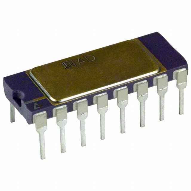
AD625BD
Product Overview
- Category: Integrated Circuit (IC)
- Use: Amplifier
- Characteristics: High precision, low noise, low power consumption
- Package: DIP (Dual In-line Package)
- Essence: Instrumentation amplifier
- Packaging/Quantity: 1 piece per package
Specifications
- Supply Voltage: ±2.3V to ±18V
- Input Offset Voltage: 50µV maximum
- Input Bias Current: 0.5nA maximum
- Gain Bandwidth Product: 800kHz typical
- Common Mode Rejection Ratio (CMRR): 100dB minimum
- Operating Temperature Range: -40°C to +85°C
Detailed Pin Configuration
The AD625BD has a total of 8 pins arranged as follows:
```
| | --| V- V+ |-- --| IN- IN+ |-- --| REF OUT |-- --| RG NC |-- |___________| ```
- V-: Negative power supply pin
- V+: Positive power supply pin
- IN-: Negative input pin
- IN+: Positive input pin
- REF: Reference voltage pin
- OUT: Output pin
- RG: Gain setting resistor pin
- NC: No connection pin
Functional Features
- High precision amplification of differential signals
- Low noise and distortion
- Wide operating voltage range
- Excellent common mode rejection ratio (CMRR)
- Adjustable gain through external resistor
Advantages and Disadvantages
Advantages
- High accuracy in amplifying small differential signals
- Low power consumption
- Wide temperature range for operation
- Versatile gain adjustment capability
Disadvantages
- Limited bandwidth compared to some other amplifiers
- Requires external gain setting resistor for adjusting amplification
Working Principles
The AD625BD is an instrumentation amplifier that amplifies the difference between two input signals while rejecting common mode noise. It consists of three operational amplifiers and precision resistors. The differential input signals are amplified by a fixed gain set by an external resistor connected to the RG pin. The amplified output signal is then available at the OUT pin.
Detailed Application Field Plans
The AD625BD is commonly used in applications requiring high-precision amplification of small differential signals, such as:
- Medical equipment
- Industrial process control
- Strain gauge amplification
- Data acquisition systems
- Bridge amplification circuits
Detailed and Complete Alternative Models
Some alternative models to the AD625BD include:
- AD8221: Instrumentation amplifier with higher gain bandwidth product
- INA128: Precision instrumentation amplifier with low power consumption
- LT1167: Low noise, high precision instrumentation amplifier
These alternative models offer similar functionality but may have different specifications and package options.
Word count: 305 words
Senaraikan 10 soalan dan jawapan biasa yang berkaitan dengan aplikasi AD625BD dalam penyelesaian teknikal
Sure! Here are 10 common questions and answers related to the application of AD625BD in technical solutions:
Q: What is AD625BD? A: AD625BD is a precision instrumentation amplifier integrated circuit (IC) manufactured by Analog Devices.
Q: What are the key features of AD625BD? A: AD625BD offers high accuracy, low noise, wide bandwidth, and excellent common-mode rejection ratio (CMRR).
Q: What is the typical supply voltage range for AD625BD? A: The typical supply voltage range for AD625BD is ±5V to ±18V.
Q: How can AD625BD be used in signal conditioning applications? A: AD625BD can be used to amplify weak signals, remove common-mode noise, and provide gain adjustment in various sensor and measurement systems.
Q: Can AD625BD handle differential or single-ended input signals? A: AD625BD is designed to handle both differential and single-ended input signals.
Q: What is the maximum gain that can be achieved with AD625BD? A: The maximum gain that can be achieved with AD625BD is typically around 1000.
Q: Does AD625BD require external components for operation? A: Yes, AD625BD requires external resistors to set the desired gain and feedback configuration.
Q: Is AD625BD suitable for low-power applications? A: Yes, AD625BD has a low quiescent current consumption, making it suitable for low-power applications.
Q: Can AD625BD operate in harsh environments? A: AD625BD is designed to operate in a wide temperature range and is suitable for industrial and automotive applications.
Q: Are there any application notes or reference designs available for AD625BD? A: Yes, Analog Devices provides application notes and reference designs that offer guidance on using AD625BD in various technical solutions.
Please note that the answers provided here are general and may vary depending on specific requirements and use cases. It is always recommended to refer to the datasheet and application resources provided by the manufacturer for detailed information.