

ADN2813ACPZ
Overview
Category
ADN2813ACPZ belongs to the category of integrated circuits (ICs).
Use
It is primarily used in electronic devices for signal processing and communication applications.
Characteristics
- High-performance integrated circuit
- Designed for signal processing and communication purposes
- Compact size and low power consumption
- Reliable and durable
Package
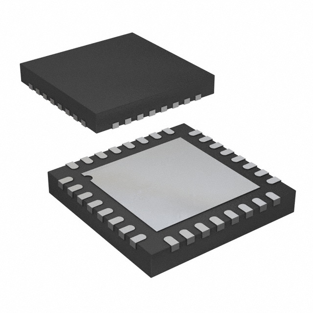
ADN2813ACPZ comes in a small form factor package, specifically the LFCSP (Lead Frame Chip Scale Package) package.
Essence
The essence of ADN2813ACPZ lies in its ability to process signals efficiently and accurately, enabling seamless communication in electronic devices.
Packaging/Quantity
Each package of ADN2813ACPZ contains one unit of the integrated circuit.
Specifications and Parameters
- Input voltage range: 2.7V - 3.6V
- Operating temperature: -40°C to +85°C
- Data rate: Up to 2.5 Gbps
- Power consumption: Low power consumption design
- Output impedance: 50 ohms
- Supply current: 100 mA (typical)
Pin Configuration
The pin configuration of ADN2813ACPZ is as follows:
- VCC
- GND
- RXIN
- RXIP
- RXVN
- RXVP
- TXOUTP
- TXOUTN
- TXINP
- TXINN
Functional Characteristics
ADN2813ACPZ offers the following functional characteristics:
- Signal amplification and conditioning
- Clock and data recovery
- Equalization and synchronization
- Noise reduction and filtering
- Differential input and output
Advantages and Disadvantages
Advantages
- High-performance signal processing capabilities
- Compact size for easy integration into various devices
- Low power consumption for energy efficiency
- Reliable and durable design for long-term use
Disadvantages
- Limited compatibility with certain device architectures
- Higher cost compared to some alternative models
Applicable Range of Products
ADN2813ACPZ is suitable for a wide range of products, including:
- Optical communication systems
- Data transmission equipment
- Networking devices
- High-speed data processing applications
Working Principles
The working principle of ADN2813ACPZ involves the following steps:
- Signal input: The integrated circuit receives the input signal from the external source.
- Signal conditioning: The signal is amplified, equalized, and synchronized to ensure optimal quality.
- Clock and data recovery: The circuit extracts the clock and data information from the input signal.
- Noise reduction: The integrated circuit filters out noise and interference for improved signal integrity.
- Signal output: The processed signal is then transmitted to the output interface.
Detailed Application Field Plans
ADN2813ACPZ can be applied in various fields, such as:
- Telecommunications: Used in optical communication systems for reliable data transmission.
- Networking: Integrated into networking devices to enhance signal processing capabilities.
- Data centers: Employed in high-speed data processing applications for efficient data transfer.
- Broadcasting: Utilized in broadcasting equipment to ensure clear and accurate signal reception.
- Industrial automation: Incorporated into industrial control systems for reliable communication between devices.
Detailed Alternative Models
Some alternative models to ADN2813ACPZ include:
- ADN2814ACPZ
- ADN2815ACPZ
- ADN2816ACPZ
- ADN2817ACPZ
- ADN2818ACPZ
5 Common Technical Questions and Answers
Q: What is the maximum data rate supported by ADN2813ACPZ? A: ADN2813ACPZ supports data rates of up to 2.5 Gbps.
Q: What is the operating temperature range for this integrated circuit? A: The operating temperature range for ADN2813ACPZ is -40°C to +85°C.
Q: Can ADN2813ACPZ be used in networking devices? A: Yes, ADN2813ACPZ is suitable for integration into networking devices for enhanced signal processing capabilities.
Q: Does ADN2813ACPZ require a specific power supply voltage? A: Yes, it requires an input voltage range of 2.7V to 3.6V.
Q: What is the output impedance of ADN2813ACPZ? A: The output impedance is 50 ohms.
This encyclopedia entry provides an overview of ADN2813ACPZ, including its category, use, characteristics, package, specifications, pin configuration, functional characteristics, advantages and disadvantages, applicable range of products, working principles, detailed application field plans, alternative models, and common technical