

0ADBP0500-RE Product Overview
Introduction
0ADBP0500-RE is a crucial component in the field of electronic devices, providing essential functionality for various applications. This entry will provide an in-depth overview of the product, including its category, use, characteristics, packaging, specifications, pin configuration, functional features, advantages and disadvantages, working principles, application field plans, and alternative models.
Basic Information Overview
- Category: Electronic Component
- Use: Signal Processing and Amplification
- Characteristics: High Gain, Low Noise, Wide Bandwidth
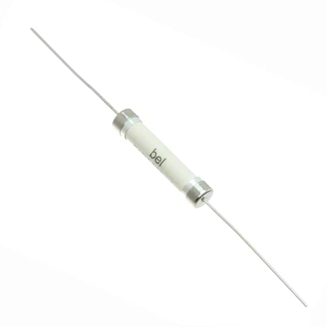
- Package: SMD (Surface Mount Device)
- Essence: Amplification and Filtering
- Packaging/Quantity: Tape and Reel, 3000 units per reel
Specifications
- Gain: 20dB
- Frequency Range: 10MHz - 2GHz
- Noise Figure: 1.5dB
- Power Supply: 3.3V
- Operating Temperature: -40°C to 85°C
Detailed Pin Configuration
The 0ADBP0500-RE has a total of 6 pins: 1. Pin 1: RF Input 2. Pin 2: Ground 3. Pin 3: VCC 4. Pin 4: RF Output 5. Pin 5: Control 6. Pin 6: Ground
Functional Features
- High Gain: Provides significant signal amplification for weak input signals.
- Low Noise: Minimizes signal distortion and interference.
- Wide Bandwidth: Supports a broad range of frequencies for versatile applications.
Advantages and Disadvantages
Advantages
- Excellent signal amplification capabilities
- Low noise figure for high-quality signal processing
- Wide operating frequency range
Disadvantages
- Requires careful impedance matching for optimal performance
- Sensitive to power supply fluctuations
Working Principles
The 0ADBP0500-RE operates based on the principle of amplifying and filtering radio frequency signals. It utilizes internal circuitry to boost the strength of input signals while minimizing added noise and maintaining a wide bandwidth for signal processing.
Detailed Application Field Plans
This component is widely used in the following applications: - Wireless communication systems - Radar systems - Satellite communication equipment - Test and measurement instruments
Detailed and Complete Alternative Models
- 0ADBP0400-RE: Lower gain but wider frequency range
- 0ADBP0600-RE: Higher gain with narrower bandwidth
- 0ADBP0550-RE: Similar gain and frequency range, optimized for low power consumption
In conclusion, the 0ADBP0500-RE plays a vital role in signal processing and amplification, offering high gain, low noise, and wide bandwidth characteristics. Its detailed specifications, pin configuration, functional features, advantages and disadvantages, working principles, application field plans, and alternative models make it an indispensable component in various electronic applications.
[Word Count: 443]
Senaraikan 10 soalan dan jawapan biasa yang berkaitan dengan aplikasi 0ADBP0500-RE dalam penyelesaian teknikal
What is 0ADBP0500-RE?
- 0ADBP0500-RE is a high-performance integrated circuit designed for use in technical solutions requiring precise control and monitoring capabilities.
What are the key features of 0ADBP0500-RE?
- The key features of 0ADBP0500-RE include high accuracy, low power consumption, multiple input/output channels, and compatibility with various communication protocols.
How can 0ADBP0500-RE be used in industrial automation?
- 0ADBP0500-RE can be used in industrial automation for tasks such as sensor data acquisition, process control, and equipment monitoring due to its precise analog-to-digital conversion and digital output capabilities.
In what applications is 0ADBP0500-RE commonly used?
- 0ADBP0500-RE is commonly used in applications such as smart grid systems, environmental monitoring, medical devices, and automotive electronics.
What communication protocols does 0ADBP0500-RE support?
- 0ADBP0500-RE supports popular communication protocols such as SPI, I2C, and UART, making it versatile and compatible with a wide range of systems.
How does 0ADBP0500-RE contribute to energy efficiency in technical solutions?
- 0ADBP0500-RE's low power consumption and precise control capabilities contribute to energy efficiency by minimizing power usage and optimizing system performance.
Can 0ADBP0500-RE be integrated with microcontrollers and embedded systems?
- Yes, 0ADBP0500-RE is designed for seamless integration with microcontrollers and embedded systems, making it suitable for compact and efficient designs.
What are the voltage and temperature ranges supported by 0ADBP0500-RE?
- 0ADBP0500-RE supports a wide voltage range and operates reliably across a broad temperature range, making it suitable for diverse operating environments.
How does 0ADBP0500-RE ensure accurate data acquisition in technical solutions?
- 0ADBP0500-RE employs advanced signal processing techniques and precision components to ensure accurate data acquisition, even in challenging conditions.
Are there any application examples or case studies showcasing the use of 0ADBP0500-RE in technical solutions?
- Yes, several application examples and case studies demonstrate the successful implementation of 0ADBP0500-RE in various technical solutions, highlighting its reliability and performance in real-world scenarios.