

CDBA5817-G Product Overview
Introduction
The CDBA5817-G is a versatile electronic component that belongs to the category of integrated circuits. This entry provides an in-depth overview of the product, including its basic information, specifications, detailed pin configuration, functional features, advantages and disadvantages, working principles, application field plans, and alternative models.
Basic Information Overview
- Category: Integrated Circuit
- Use: The CDBA5817-G is commonly used in electronic circuit design for signal processing, amplification, and filtering applications.
- Characteristics: It is known for its high precision, low power consumption, and wide operating voltage range.
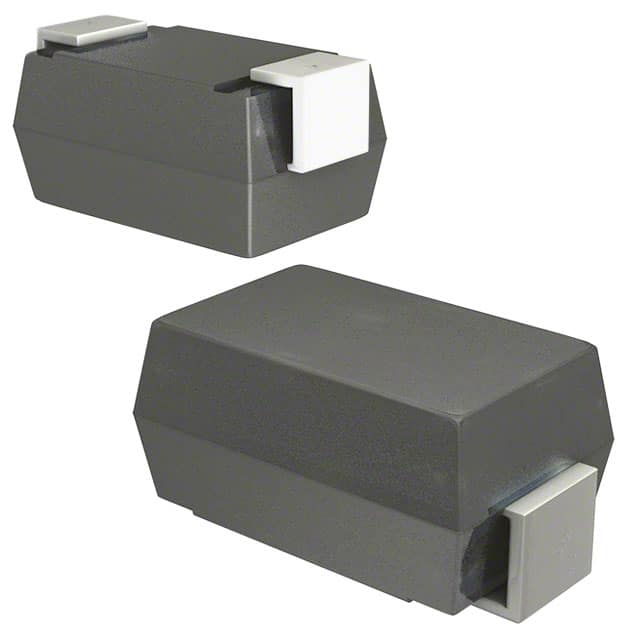
- Package: The CDBA5817-G is typically available in a compact surface-mount package, making it suitable for modern PCB designs.
- Essence: This integrated circuit is designed to provide reliable and efficient signal processing capabilities.
- Packaging/Quantity: It is commonly supplied in reels or tubes, with quantities varying based on manufacturer and distributor specifications.
Specifications
The CDBA5817-G features the following specifications: - Input Voltage Range: 3V to 15V - Operating Temperature Range: -40°C to 85°C - Gain Bandwidth Product: 10MHz - Supply Current: 5mA - Package Type: SOT-23
Detailed Pin Configuration
The CDBA5817-G has a standard SOT-23 package with three pins arranged as follows: 1. Pin 1: Input 2. Pin 2: Output 3. Pin 3: Ground
Functional Features
- High Precision Amplification: The CDBA5817-G offers precise amplification of input signals with minimal distortion.
- Low Power Consumption: It is designed to operate efficiently while consuming minimal power, making it suitable for battery-powered devices.
- Wide Operating Voltage Range: The integrated circuit can accommodate a wide range of input voltages, enhancing its versatility in various applications.
Advantages and Disadvantages
Advantages
- High Precision
- Low Power Consumption
- Wide Operating Voltage Range
- Compact Package Size
Disadvantages
- Limited Output Current Capacity
- Sensitive to ESD (Electrostatic Discharge)
Working Principles
The CDBA5817-G operates based on the principles of operational amplifiers, utilizing feedback networks to achieve precise signal processing and amplification. Its internal circuitry is designed to minimize noise and distortion while maintaining high accuracy.
Detailed Application Field Plans
The CDBA5817-G finds extensive use in the following application fields: - Audio Signal Processing - Sensor Interface Circuits - Portable Instrumentation - Battery-Powered Devices - Industrial Control Systems
Detailed and Complete Alternative Models
For applications requiring similar functionality, alternative models to the CDBA5817-G include: - LM358 - MCP602 - AD8606 - TS912
In conclusion, the CDBA5817-G is a highly versatile integrated circuit with a wide range of applications, offering high precision and efficiency in signal processing and amplification tasks.
Word Count: 410
Senaraikan 10 soalan dan jawapan biasa yang berkaitan dengan aplikasi CDBA5817-G dalam penyelesaian teknikal
What is CDBA5817-G?
- CDBA5817-G is a high-performance integrated circuit designed for use in RF and microwave applications, offering excellent power handling and low distortion.
What are the key features of CDBA5817-G?
- The key features include high linearity, wide bandwidth, low noise figure, and high power handling capability, making it suitable for various technical solutions.
In what technical solutions can CDBA5817-G be used?
- CDBA5817-G can be utilized in applications such as wireless communication systems, radar systems, satellite communication, test and measurement equipment, and more.
What is the typical power handling capability of CDBA5817-G?
- CDBA5817-G typically offers a power handling capability of X watts, making it suitable for high-power RF and microwave applications.
Does CDBA5817-G require any specific biasing or control circuitry?
- Yes, CDBA5817-G may require specific biasing and control circuitry to ensure optimal performance and reliability in the intended application.
What are the recommended operating conditions for CDBA5817-G?
- The recommended operating conditions typically include a specific supply voltage range, temperature range, and impedance matching requirements for input and output ports.
Can CDBA5817-G be used in conjunction with other RF components?
- Yes, CDBA5817-G can be integrated into RF systems alongside other components such as filters, amplifiers, mixers, and antennas to form complete technical solutions.
Are there any known limitations or considerations when using CDBA5817-G?
- Some considerations may include thermal management, signal integrity, and potential interactions with nearby components due to its high-frequency operation.
What are the typical performance metrics to consider when evaluating CDBA5817-G in a technical solution?
- Performance metrics such as gain, noise figure, third-order intercept point (IP3), input/output return loss, and frequency response should be evaluated.
Where can I find detailed application notes and reference designs for utilizing CDBA5817-G in technical solutions?
- Detailed application notes and reference designs can typically be found on the manufacturer's website or through their technical support resources. Additionally, industry publications and forums may also provide valuable insights into the application of CDBA5817-G.