

CY37128P84-125JXI
Product Overview
Category
CY37128P84-125JXI belongs to the category of programmable logic devices (PLDs).
Use
It is primarily used for digital circuit design and implementation in various electronic systems.
Characteristics
- High-performance PLD with advanced features
- Offers flexibility and versatility in circuit design
- Provides efficient logic functions and signal processing capabilities
Package
CY37128P84-125JXI comes in a compact and durable package, ensuring protection during handling and installation.
Essence
The essence of CY37128P84-125JXI lies in its ability to provide a customizable and reconfigurable logic solution for complex digital designs.
Packaging/Quantity
This product is typically packaged in trays or tubes, with each containing a specific quantity of CY37128P84-125JXI units.
Specifications
- Model: CY37128P84-125JXI
- Logic Elements: 128 macrocells
- Maximum Operating Frequency: 125 MHz
- Supply Voltage: 3.3V
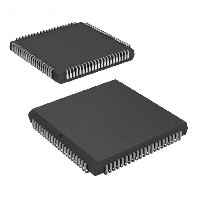
- Package Type: 84-pin PLCC
Detailed Pin Configuration
The pin configuration of CY37128P84-125JXI is as follows:
- VCCIO
- GND
- I/O0
- I/O1
- I/O2
- I/O3
- I/O4
- I/O5
- I/O6
- I/O7
- I/O8
- I/O9
- I/O10
- I/O11
- I/O12
- I/O13
- I/O14
- I/O15
- I/O16
- I/O17
- I/O18
- I/O19
- I/O20
- I/O21
- I/O22
- I/O23
- I/O24
- I/O25
- I/O26
- I/O27
- I/O28
- I/O29
- I/O30
- I/O31
- I/O32
- I/O33
- I/O34
- I/O35
- I/O36
- I/O37
- I/O38
- I/O39
- I/O40
- I/O41
- I/O42
- I/O43
- I/O44
- I/O45
- I/O46
- I/O47
- I/O48
- I/O49
- I/O50
- I/O51
- I/O52
- I/O53
- I/O54
- I/O55
- I/O56
- I/O57
- I/O58
- I/O59
- I/O60
- I/O61
- I/O62
- I/O63
- I/O64
- I/O65
- I/O66
- I/O67
- I/O68
- I/O69
- I/O70
- I/O71
- I/O72
- I/O73
- I/O74
- I/O75
- I/O76
- I/O77
- I/O78
- I/O79
- I/O80
- I/O81
Functional Features
- High-speed and efficient logic processing
- Configurable macrocells for custom logic implementation
- Flexible input/output configurations
- Support for various digital interfaces and protocols
Advantages and Disadvantages
Advantages
- Versatile and customizable logic solution
- High-performance capabilities
- Efficient utilization of resources
- Wide range of application possibilities
Disadvantages
- Limited number of macrocells compared to higher-end PLDs
- Higher power consumption compared to some low-power alternatives
Working Principles
CY37128P84-125JXI operates based on the principles of programmable logic. It consists of configurable logic blocks (CLBs) that can be programmed to implement desired logic functions. The device is programmed using a hardware description language (HDL) or a graphical design tool, which generates a configuration file. This file is then loaded into the PLD, configuring it to perform the desired logic operations.
Detailed Application Field Plans
CY37128P84-125JXI finds applications in various fields, including:
- Industrial automation
- Telecommunications
- Consumer electronics
- Automotive systems
- Medical devices
Senaraikan 10 soalan dan jawapan biasa yang berkaitan dengan aplikasi CY37128P84-125JXI dalam penyelesaian teknikal
Sure! Here are 10 common questions and answers related to the application of CY37128P84-125JXI in technical solutions:
Q: What is CY37128P84-125JXI? A: CY37128P84-125JXI is a programmable logic device (PLD) manufactured by Cypress Semiconductor. It offers high-density, low-power, and high-performance capabilities.
Q: What are the key features of CY37128P84-125JXI? A: Some key features include 128 macrocells, 84 pins, 125 MHz maximum operating frequency, JTAG programming interface, and 3.3V power supply.
Q: In what applications can CY37128P84-125JXI be used? A: CY37128P84-125JXI can be used in various applications such as telecommunications, industrial automation, consumer electronics, automotive systems, and more.
Q: How does CY37128P84-125JXI differ from other PLDs? A: CY37128P84-125JXI stands out due to its high-density architecture, low power consumption, and high-speed performance, making it suitable for complex designs.
Q: What programming options are available for CY37128P84-125JXI? A: CY37128P84-125JXI can be programmed using industry-standard programming tools like the Cypress Warp software or third-party programming tools compatible with JTAG interface.
Q: Can CY37128P84-125JXI be reprogrammed after initial programming? A: Yes, CY37128P84-125JXI supports in-system programming (ISP), allowing for reprogramming without removing the device from the circuit.
Q: What are the voltage requirements for CY37128P84-125JXI? A: CY37128P84-125JXI operates on a 3.3V power supply, making it compatible with standard digital logic levels.
Q: What is the maximum operating frequency of CY37128P84-125JXI? A: The maximum operating frequency of CY37128P84-125JXI is 125 MHz, enabling high-speed data processing and real-time applications.
Q: Can CY37128P84-125JXI interface with other components or microcontrollers? A: Yes, CY37128P84-125JXI can interface with other components or microcontrollers using various communication protocols such as SPI, I2C, UART, etc.
Q: Are there any development tools or resources available for working with CY37128P84-125JXI? A: Yes, Cypress Semiconductor provides development tools like the Warp software, datasheets, application notes, and technical support to assist in designing with CY37128P84-125JXI.
Please note that the answers provided here are general and may vary based on specific requirements and design considerations.