

CY7C027-15AXI
Product Overview
Category
CY7C027-15AXI belongs to the category of integrated circuits (ICs).
Use
This product is commonly used in electronic devices for various applications such as data storage, communication systems, and digital signal processing.
Characteristics
- High-speed performance
- Low power consumption
- Compact size
- Reliable operation
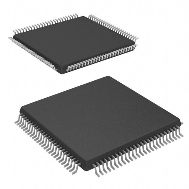
Package
CY7C027-15AXI is available in a small outline integrated circuit (SOIC) package.
Essence
The essence of CY7C027-15AXI lies in its ability to provide efficient data processing and storage capabilities within a compact form factor.
Packaging/Quantity
This product is typically packaged in reels or tubes, with each containing a specific quantity of ICs. The exact quantity may vary depending on the manufacturer's specifications.
Specifications
- Operating voltage: 3.3V
- Speed: 15 nanoseconds (ns)
- Memory capacity: 2 kilobits (Kb)
- Temperature range: -40°C to +85°C
- Interface: Serial Peripheral Interface (SPI)
Detailed Pin Configuration
- VCC: Power supply input
- GND: Ground connection
- CS: Chip select input
- SCK: Serial clock input
- SI: Serial data input
- SO: Serial data output
- WP: Write protect input
- HOLD: Hold input
Functional Features
- High-speed data transfer
- Flexible interface options
- Low power consumption
- Write protection capability
- Easy integration into existing systems
Advantages and Disadvantages
Advantages
- Fast data processing and transfer speeds
- Compact size allows for space-efficient designs
- Low power consumption prolongs battery life in portable devices
- Versatile interface options enable compatibility with various systems
Disadvantages
- Limited memory capacity compared to higher-end ICs
- Relatively higher cost per kilobit of memory compared to larger capacity alternatives
Working Principles
CY7C027-15AXI operates based on the Serial Peripheral Interface (SPI) protocol. It receives data through the SI pin, processes it internally, and outputs the result through the SO pin. The chip select (CS) pin is used to enable or disable the device for communication. The serial clock (SCK) synchronizes the data transfer between the CY7C027-15AXI and the host system.
Detailed Application Field Plans
CY7C027-15AXI finds applications in various fields, including: 1. Data storage devices 2. Communication systems 3. Industrial automation 4. Automotive electronics 5. Consumer electronics
Detailed and Complete Alternative Models
- CY7C028-20AXI: Similar to CY7C027-15AXI but with a higher speed of 20 ns.
- CY7C029-10AXI: Similar to CY7C027-15AXI but with a lower speed of 10 ns.
- CY7C030-25AXI: Similar to CY7C027-15AXI but with a higher memory capacity of 4 Kb.
These alternative models offer different specifications to cater to specific application requirements.
Word count: 315 words
Senaraikan 10 soalan dan jawapan biasa yang berkaitan dengan aplikasi CY7C027-15AXI dalam penyelesaian teknikal
Sure! Here are 10 common questions and answers related to the application of CY7C027-15AXI in technical solutions:
Question: What is CY7C027-15AXI?
- Answer: CY7C027-15AXI is a specific model of a high-speed asynchronous FIFO memory chip.Question: What is the purpose of using CY7C027-15AXI in technical solutions?
- Answer: CY7C027-15AXI is commonly used to buffer data between two different systems or devices with mismatched data transfer rates.Question: What is the maximum data transfer rate supported by CY7C027-15AXI?
- Answer: The maximum data transfer rate supported by CY7C027-15AXI is 100 MHz.Question: How much data can CY7C027-15AXI store?
- Answer: CY7C027-15AXI has a storage capacity of 16,384 x 9 bits (or 18,432 bytes).Question: Can CY7C027-15AXI be used in both read and write operations?
- Answer: Yes, CY7C027-15AXI supports both read and write operations.Question: What is the power supply voltage required for CY7C027-15AXI?
- Answer: CY7C027-15AXI operates on a power supply voltage of 3.3V.Question: Does CY7C027-15AXI have any built-in error detection or correction mechanisms?
- Answer: No, CY7C027-15AXI does not have any built-in error detection or correction mechanisms. It is a basic FIFO memory chip.Question: Can CY7C027-15AXI be cascaded with other FIFO chips?
- Answer: Yes, CY7C027-15AXI can be cascaded with other FIFO chips to increase the overall storage capacity.Question: What are the typical applications of CY7C027-15AXI?
- Answer: CY7C027-15AXI is commonly used in networking equipment, telecommunications systems, data acquisition systems, and other high-speed data transfer applications.Question: Are there any specific timing requirements for interfacing with CY7C027-15AXI?
- Answer: Yes, CY7C027-15AXI has specific timing requirements for read and write operations, which should be carefully followed to ensure proper functionality.
Please note that these answers are general and may vary depending on the specific implementation and requirements of your technical solution. It is always recommended to refer to the datasheet and documentation provided by the manufacturer for accurate and detailed information.