

Encyclopedia Entry: 74LVC1G08FZ4-7
Product Overview
The 74LVC1G08FZ4-7 is an integrated circuit (IC) belonging to the category of logic gates. It is specifically designed for use in digital electronics applications. This IC serves as a single 2-input AND gate, making it an essential component in various electronic circuits.
Characteristics
- Category: Logic Gates
- Use: Digital Electronics
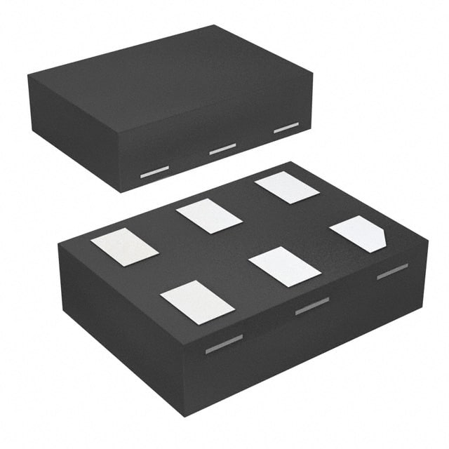
- Package: SOT-353
- Essence: Single 2-input AND Gate
- Packaging/Quantity: Tape and Reel, 3000 pieces per reel
Specifications
- Supply Voltage Range: 1.65V to 5.5V
- High-Level Input Voltage: 0.7 x VCC
- Low-Level Input Voltage: 0.3 x VCC
- High-Level Output Current: -32mA
- Low-Level Output Current: 32mA
- Propagation Delay: 4.3ns (typical)
Detailed Pin Configuration
The 74LVC1G08FZ4-7 IC has a total of 5 pins, each serving a specific function: 1. Pin 1: Input A 2. Pin 2: Input B 3. Pin 3: Ground (GND) 4. Pin 4: Output Y 5. Pin 5: Power Supply (VCC)
Functional Features
- Single 2-input AND gate functionality
- Wide supply voltage range allows compatibility with various systems
- High-speed operation with low propagation delay
- Balanced output drive capability for improved noise immunity
- Schmitt-trigger input for hysteresis and increased noise tolerance
Advantages and Disadvantages
Advantages: - Compact size and low power consumption - Versatile application possibilities - Excellent noise immunity due to Schmitt-trigger input
Disadvantages: - Limited number of inputs (2-input only) - Not suitable for complex logic operations requiring multiple gates
Working Principles
The 74LVC1G08FZ4-7 operates based on the principles of Boolean logic. It performs the logical AND operation on its two input signals, A and B, and produces a corresponding output signal, Y. The IC utilizes transistors and other electronic components to achieve this functionality.
Detailed Application Field Plans
The 74LVC1G08FZ4-7 finds extensive use in various digital electronics applications, including but not limited to: - Microcontrollers and microprocessors - Data communication systems - Industrial automation - Consumer electronics - Automotive electronics
Detailed Alternative Models
For those seeking alternative options, several similar ICs can be considered as replacements or alternatives to the 74LVC1G08FZ4-7. Some notable alternatives include: - SN74LVC1G08DBVR - MC74VHC1G08DTT1G - TC7SZ08FU
These alternatives offer similar functionality and characteristics, providing flexibility in design choices.
In conclusion, the 74LVC1G08FZ4-7 is a compact and versatile logic gate IC widely used in digital electronics applications. Its single 2-input AND gate functionality, along with its excellent noise immunity and low power consumption, make it an essential component in various electronic circuits.
Senaraikan 10 soalan dan jawapan biasa yang berkaitan dengan aplikasi 74LVC1G08FZ4-7 dalam penyelesaian teknikal
Sure! Here are 10 common questions and answers related to the application of the 74LVC1G08FZ4-7 in technical solutions:
Q1: What is the 74LVC1G08FZ4-7? A1: The 74LVC1G08FZ4-7 is a single 2-input AND gate IC (integrated circuit) that operates at 3.3V or 5V supply voltage.
Q2: What is the purpose of an AND gate? A2: An AND gate is a logic gate that produces a high output only when all its inputs are high.
Q3: What are the typical applications of the 74LVC1G08FZ4-7? A3: The 74LVC1G08FZ4-7 can be used in various applications such as signal conditioning, level shifting, data routing, and general-purpose logic functions.
Q4: What is the maximum operating frequency of the 74LVC1G08FZ4-7? A4: The maximum operating frequency of the 74LVC1G08FZ4-7 is typically around 500 MHz.
Q5: What is the input voltage range for the 74LVC1G08FZ4-7? A5: The input voltage range for the 74LVC1G08FZ4-7 is from ground (0V) to the supply voltage (3.3V or 5V).
Q6: Can the 74LVC1G08FZ4-7 handle multiple power supplies? A6: No, the 74LVC1G08FZ4-7 is designed to operate with a single power supply.
Q7: What is the output drive capability of the 74LVC1G08FZ4-7? A7: The 74LVC1G08FZ4-7 has a typical output drive capability of 32 mA.
Q8: Can the 74LVC1G08FZ4-7 be used in both CMOS and TTL logic systems? A8: Yes, the 74LVC1G08FZ4-7 is compatible with both CMOS and TTL logic levels.
Q9: Is the 74LVC1G08FZ4-7 available in different package options? A9: Yes, the 74LVC1G08FZ4-7 is available in various package options such as SOT353, SC-88A, and XSON6.
Q10: What are the temperature range and storage conditions for the 74LVC1G08FZ4-7? A10: The operating temperature range for the 74LVC1G08FZ4-7 is typically -40°C to +125°C, and it should be stored in a dry environment at temperatures between -55°C and +150°C.
Please note that the answers provided here are general and may vary depending on the specific datasheet and manufacturer's specifications for the 74LVC1G08FZ4-7.