

Encyclopedia Entry: 74LVC1G125FZ4-7
Product Overview
- Category: Integrated Circuit (IC)
- Use: Logic Level Shifter
- Characteristics: High-speed, low-power, single gate buffer with voltage level translation capability
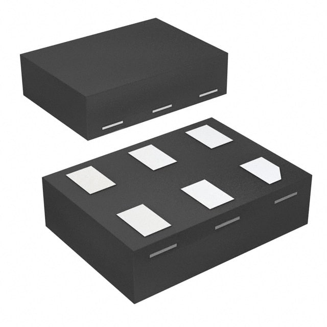
- Package: SOT353 (SC-88A), 5-pin package
- Essence: Single gate buffer with tri-state output and voltage level shifting capabilities
- Packaging/Quantity: Tape and Reel, 3000 units per reel
Specifications
- Supply Voltage Range: 1.65V to 5.5V
- Input Voltage Range (V_I): GND to V_CC
- Output Voltage Range (V_O): GND to V_CC
- Maximum Input Current (I_I): ±24mA
- Maximum Output Current (I_O): ±32mA
- Propagation Delay (t_PD): 3.8ns (typical) at VCC = 3.3V, TA = 25°C
- Operating Temperature Range: -40°C to +125°C
Detailed Pin Configuration
The 74LVC1G125FZ4-7 has the following pin configuration:
____
   OE --|    |-- V_CC
   A  --|    |-- Y
 GND --|    |-- A
   B  --|    |-- OE
        ----
Functional Features
- Single gate buffer with tri-state output
- Provides voltage level shifting between different logic levels
- Supports bidirectional data flow
- Low power consumption
- High-speed operation
Advantages
- Small form factor package allows for space-saving designs
- Wide supply voltage range enables compatibility with various systems
- Tri-state output allows for easy bus sharing and interfacing with multiple devices
- Low propagation delay ensures fast signal transmission
Disadvantages
- Limited number of input/output pins (single gate)
- Not suitable for high-current applications
- Sensitive to electrostatic discharge (ESD) due to small package size
Working Principles
The 74LVC1G125FZ4-7 is a single gate buffer that operates as a voltage level shifter. It accepts logic level inputs from one voltage domain and translates them to another voltage domain, allowing seamless communication between different logic families or systems. The tri-state output feature enables the device to be easily connected to a shared bus, where multiple devices can drive the bus lines without conflict.
Detailed Application Field Plans
The 74LVC1G125FZ4-7 finds applications in various fields, including: 1. Consumer electronics: Mobile phones, tablets, and portable devices requiring voltage level translation between different components. 2. Industrial automation: PLCs (Programmable Logic Controllers), sensors, and actuators that operate at different logic levels. 3. Automotive electronics: ECU (Engine Control Unit), infotainment systems, and body control modules requiring voltage level shifting for communication between different subsystems. 4. Communication systems: Routers, switches, and network equipment that interface with different logic families or voltage domains.
Detailed and Complete Alternative Models
- SN74LVC1G125DBVR - Texas Instruments
- MC74VHC1GT125DF1G - ON Semiconductor
- NC7SZ125P5X - Fairchild Semiconductor
- TC7SZ125FU - Toshiba Semiconductor
These alternative models offer similar functionality and can be used as replacements for the 74LVC1G125FZ4-7 in various applications.
Word count: 440 words
Senaraikan 10 soalan dan jawapan biasa yang berkaitan dengan aplikasi 74LVC1G125FZ4-7 dalam penyelesaian teknikal
Sure! Here are 10 common questions and answers related to the application of 74LVC1G125FZ4-7 in technical solutions:
Q1: What is the 74LVC1G125FZ4-7? A1: The 74LVC1G125FZ4-7 is a single bus buffer gate with 3-state output, designed for low voltage applications.
Q2: What is the operating voltage range of the 74LVC1G125FZ4-7? A2: The operating voltage range is from 1.65V to 5.5V.
Q3: What is the maximum output current of the 74LVC1G125FZ4-7? A3: The maximum output current is 32mA.
Q4: Can the 74LVC1G125FZ4-7 be used as a level shifter? A4: Yes, the 74LVC1G125FZ4-7 can be used as a level shifter between different voltage domains.
Q5: How many inputs does the 74LVC1G125FZ4-7 have? A5: The 74LVC1G125FZ4-7 has one input.
Q6: How many outputs does the 74LVC1G125FZ4-7 have? A6: The 74LVC1G125FZ4-7 has one output.
Q7: What is the propagation delay of the 74LVC1G125FZ4-7? A7: The propagation delay is typically 3.8ns.
Q8: Can the 74LVC1G125FZ4-7 be used in high-speed applications? A8: Yes, the 74LVC1G125FZ4-7 is suitable for high-speed applications.
Q9: Is the 74LVC1G125FZ4-7 compatible with other logic families? A9: Yes, the 74LVC1G125FZ4-7 is compatible with both CMOS and TTL logic families.
Q10: Can the 74LVC1G125FZ4-7 be used in battery-powered devices? A10: Yes, the 74LVC1G125FZ4-7 is designed for low power consumption and can be used in battery-powered devices.
Please note that these answers are general and may vary depending on specific application requirements.