

Encyclopedia Entry: 74LVC1G126FS3-7
Product Overview
Category
The 74LVC1G126FS3-7 belongs to the category of integrated circuits (ICs).
Use
This IC is commonly used in digital logic applications for signal amplification and level shifting.
Characteristics
- Low-voltage CMOS technology
- High-speed operation
- Wide operating voltage range
- Schmitt-trigger input
- Balanced propagation delays
- Low power consumption
Package
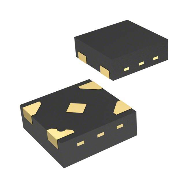
The 74LVC1G126FS3-7 is available in a small SOT-353 package, which is suitable for surface mount applications.
Essence
The essence of this product lies in its ability to provide reliable and efficient signal amplification and level shifting in various digital logic circuits.
Packaging/Quantity
The 74LVC1G126FS3-7 is typically packaged in reels or tubes, with a quantity of 3000 units per reel/tube.
Specifications
- Supply Voltage Range: 1.65V to 5.5V
- Input Voltage Range: -0.5V to VCC + 0.5V
- Output Voltage Range: 0V to VCC
- Maximum Operating Frequency: 500 MHz
- Maximum Propagation Delay: 4.3 ns
- Maximum Quiescent Current: 10 μA
Detailed Pin Configuration
The 74LVC1G126FS3-7 has the following pin configuration:
____
   OE |1  6| VCC
  AIN |2  5| Y
  GND |3  4| B
       ----
Functional Features
- Output Enable (OE) pin allows for tri-state output control.
- AIN pin serves as the input for the signal to be amplified or level-shifted.
- Y pin is the output pin, providing the amplified or level-shifted signal.
- B pin is used to control the direction of the level shifting.
Advantages and Disadvantages
Advantages
- Low power consumption makes it suitable for battery-powered devices.
- Wide operating voltage range allows for compatibility with various systems.
- High-speed operation enables efficient signal processing.
- Schmitt-trigger input ensures reliable signal detection.
Disadvantages
- Limited number of input/output pins restricts its application in complex circuits.
- Propagation delay may affect real-time applications requiring immediate response.
Working Principles
The 74LVC1G126FS3-7 operates based on CMOS technology, utilizing a combination of MOSFET transistors. The input signal is amplified or level-shifted based on the control signals applied to the OE and B pins. The amplified or level-shifted signal is then provided at the Y pin.
Detailed Application Field Plans
The 74LVC1G126FS3-7 finds extensive use in various digital logic applications, including but not limited to: - Microcontrollers - Data communication systems - Industrial automation - Consumer electronics - Automotive electronics
Detailed and Complete Alternative Models
Some alternative models that can be considered as alternatives to the 74LVC1G126FS3-7 are: - SN74LVC1G126DBVR - MC74VHC1G126DTT1G - TC7SZ126FU
These models offer similar functionality and characteristics, providing options for different design requirements.
In conclusion, the 74LVC1G126FS3-7 is a versatile integrated circuit that offers efficient signal amplification and level shifting capabilities. Its low power consumption, wide operating voltage range, and high-speed operation make it suitable for various digital logic applications. However, its limited pin count and propagation delay should be considered when selecting this IC for specific designs.
Senaraikan 10 soalan dan jawapan biasa yang berkaitan dengan aplikasi 74LVC1G126FS3-7 dalam penyelesaian teknikal
Sure! Here are 10 common questions and answers related to the application of 74LVC1G126FS3-7 in technical solutions:
Q: What is the 74LVC1G126FS3-7? A: The 74LVC1G126FS3-7 is a single bus buffer gate with three-state output, designed for low-voltage applications.
Q: What is the operating voltage range of the 74LVC1G126FS3-7? A: The operating voltage range is from 1.65V to 5.5V.
Q: What is the maximum output current of the 74LVC1G126FS3-7? A: The maximum output current is 32mA.
Q: Can the 74LVC1G126FS3-7 be used as a level shifter? A: Yes, it can be used as a level shifter to convert signals between different voltage levels.
Q: How many inputs does the 74LVC1G126FS3-7 have? A: It has one input.
Q: How many outputs does the 74LVC1G126FS3-7 have? A: It has one output.
Q: What is the propagation delay of the 74LVC1G126FS3-7? A: The typical propagation delay is 4.3ns.
Q: Can the 74LVC1G126FS3-7 be used in high-speed applications? A: Yes, it is suitable for high-speed applications due to its low propagation delay.
Q: Does the 74LVC1G126FS3-7 have a three-state output? A: Yes, it has a three-state output that can be disabled to effectively disconnect the output from the bus.
Q: What is the package type of the 74LVC1G126FS3-7? A: It comes in an SOT353 package.
Please note that these answers are based on general information about the 74LVC1G126FS3-7 and may vary depending on specific application requirements.