

74LVCE1G02FZ4
Basic Information Overview
- Category: Integrated Circuit (IC)
- Use: Logic Gate
- Characteristics: Low-voltage, high-speed, single 2-input NOR gate
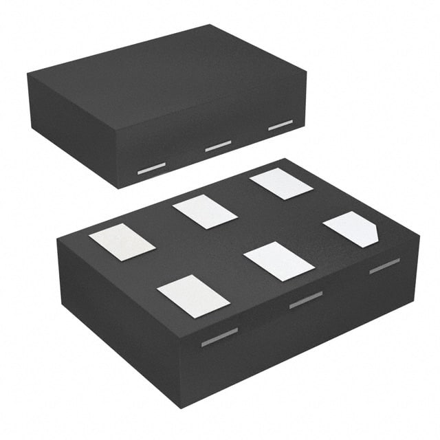
- Package: SOT-353 (SC-88A)
- Essence: Digital logic gate for logical operations
- Packaging/Quantity: Tape and Reel, 3000 pieces per reel
Specifications
- Supply Voltage Range: 1.65V to 5.5V
- Input Voltage Range: -0.5V to VCC + 0.5V
- Output Voltage Range: 0V to VCC
- Operating Temperature Range: -40°C to +125°C
- Propagation Delay: 3.6ns (typical) at 3.3V supply voltage
Detailed Pin Configuration
The 74LVCE1G02FZ4 has a total of 5 pins: 1. GND (Ground) 2. A (Input A) 3. B (Input B) 4. Y (Output) 5. VCC (Supply Voltage)
Functional Features
- Single 2-input NOR gate functionality
- Low-voltage operation allows compatibility with various systems
- High-speed operation for quick logical operations
- Schmitt-trigger input for noise immunity
- Balanced propagation delays for improved performance
Advantages and Disadvantages
Advantages: - Low-voltage operation enables integration into low-power devices - High-speed operation facilitates fast data processing - Schmitt-trigger input enhances noise immunity - Small package size saves board space
Disadvantages: - Limited number of inputs and outputs - Not suitable for complex logic operations requiring multiple gates
Working Principles
The 74LVCE1G02FZ4 is based on CMOS technology, which utilizes complementary pairs of MOSFETs (Metal-Oxide-Semiconductor Field-Effect Transistors) to implement logic functions. In this case, the NOR gate is constructed using two transistors in parallel. When both input A and input B are low (0V), the output Y becomes high (VCC). For any other combination of inputs, the output remains low (0V).
Detailed Application Field Plans
The 74LVCE1G02FZ4 can be used in various applications, including: - Digital systems requiring logical operations - Microcontrollers and microprocessors - Communication devices - Consumer electronics - Automotive electronics
Detailed and Complete Alternative Models
Some alternative models that provide similar functionality to the 74LVCE1G02FZ4 include: - SN74LVC1G02DBVR (Texas Instruments) - MC74LCX02DTG (ON Semiconductor) - NC7SZ02P5X (Fairchild Semiconductor)
Note: These alternative models may have slight differences in specifications and package options. It is recommended to refer to their respective datasheets for detailed information.
Word count: 314 words
Senaraikan 10 soalan dan jawapan biasa yang berkaitan dengan aplikasi 74LVCE1G02FZ4 dalam penyelesaian teknikal
Sure! Here are 10 common questions and answers related to the application of 74LVCE1G02FZ4 in technical solutions:
Q1: What is the 74LVCE1G02FZ4? A1: The 74LVCE1G02FZ4 is a single 2-input NOR gate IC (integrated circuit) that operates at low voltage levels.
Q2: What is the voltage range supported by the 74LVCE1G02FZ4? A2: The 74LVCE1G02FZ4 supports a voltage range from 1.65V to 5.5V.
Q3: What is the maximum operating frequency of the 74LVCE1G02FZ4? A3: The maximum operating frequency of the 74LVCE1G02FZ4 is typically around 500 MHz.
Q4: Can the 74LVCE1G02FZ4 be used as a level shifter? A4: Yes, the 74LVCE1G02FZ4 can be used as a level shifter to convert signals between different voltage levels.
Q5: How many inputs does the 74LVCE1G02FZ4 have? A5: The 74LVCE1G02FZ4 has two inputs.
Q6: What is the output logic level of the 74LVCE1G02FZ4? A6: The output logic level of the 74LVCE1G02FZ4 is compatible with both CMOS and TTL logic levels.
Q7: Can the 74LVCE1G02FZ4 be used in battery-powered applications? A7: Yes, the 74LVCE1G02FZ4 can be used in battery-powered applications due to its low power consumption.
Q8: Is the 74LVCE1G02FZ4 suitable for high-speed data transmission? A8: Yes, the 74LVCE1G02FZ4 is suitable for high-speed data transmission due to its fast propagation delay.
Q9: Can multiple 74LVCE1G02FZ4 ICs be cascaded together? A9: Yes, multiple 74LVCE1G02FZ4 ICs can be cascaded together to create more complex logic functions.
Q10: What is the package type of the 74LVCE1G02FZ4? A10: The 74LVCE1G02FZ4 is available in a small SOT-353 package.