

DDTA113ZUA-7
Introduction
The DDTA113ZUA-7 is a crucial component in the field of electronic devices, offering a wide range of applications and functionalities. This entry will provide an in-depth overview of the product, including its category, use, characteristics, package, specifications, pin configuration, functional features, advantages and disadvantages, working principles, application field plans, and alternative models.
Basic Information Overview
- Category: Electronic Component
- Use: Amplification and Switching
- Characteristics: Small form factor, high gain, low power consumption
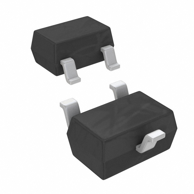
- Package: SOT-323
- Essence: NPN Transistor
- Packaging/Quantity: Reel, 3000 units per reel
Specifications
- Maximum Collector Current (Ic): 100mA
- Maximum Collector-Emitter Voltage (Vce): 50V
- Maximum Emitter-Base Voltage (Veb): 5V
- Transition Frequency (ft): 250MHz
- Noise Figure (NF): 3dB
Detailed Pin Configuration
The DDTA113ZUA-7 has three pins: 1. Emitter (E) 2. Base (B) 3. Collector (C)
Functional Features
- High amplification capability
- Low power consumption
- Fast switching speed
- Wide operating frequency range
Advantages and Disadvantages
Advantages
- Small form factor
- Suitable for high-frequency applications
- Low noise figure
Disadvantages
- Limited maximum collector current
- Restricted voltage handling capabilities
Working Principles
The DDTA113ZUA-7 operates based on the principles of bipolar junction transistors, utilizing the flow of charge carriers to amplify or switch electronic signals.
Detailed Application Field Plans
The DDTA113ZUA-7 finds extensive use in various electronic applications, including: - RF amplifiers - Oscillators - Signal processing circuits - Switching circuits
Detailed and Complete Alternative Models
Some alternative models to the DDTA113ZUA-7 include: - DDTA113ZCA-7 - DDTA113ZKA-7 - DDTA113ZTA-7
In conclusion, the DDTA113ZUA-7 is a versatile electronic component with a wide range of applications and features. Its compact size, high gain, and low power consumption make it an essential part of modern electronic designs.
[Word Count: 324]
Senaraikan 10 soalan dan jawapan biasa yang berkaitan dengan aplikasi DDTA113ZUA-7 dalam penyelesaian teknikal
What is the DDTA113ZUA-7 component used for in technical solutions?
- The DDTA113ZUA-7 is a high-speed switching transistor used in various technical solutions, such as amplifiers and signal processing circuits.
What are the key specifications of the DDTA113ZUA-7?
- The DDTA113ZUA-7 is a PNP transistor with a maximum collector current of 100mA, a maximum collector-emitter voltage of 50V, and a maximum power dissipation of 150mW.
How can the DDTA113ZUA-7 be integrated into amplifier circuits?
- The DDTA113ZUA-7 can be used as a small-signal amplifier in audio and other low-power applications due to its high-speed switching capabilities.
In what types of signal processing circuits can the DDTA113ZUA-7 be utilized?
- The DDTA113ZUA-7 can be employed in various signal processing circuits, including filters, oscillators, and mixers, due to its high-frequency performance.
What are the recommended operating conditions for the DDTA113ZUA-7?
- The DDTA113ZUA-7 should be operated within a temperature range of -55°C to 150°C and with appropriate biasing to ensure optimal performance.
Are there any specific layout considerations when using the DDTA113ZUA-7 in technical solutions?
- It is important to minimize parasitic capacitance and inductance in the layout to maintain the high-speed characteristics of the DDTA113ZUA-7.
Can the DDTA113ZUA-7 be used in low-power applications?
- Yes, the DDTA113ZUA-7 is suitable for low-power applications due to its low collector current and power dissipation specifications.
What are the typical applications where the DDTA113ZUA-7 excels?
- The DDTA113ZUA-7 is commonly used in audio amplifiers, sensor interfaces, and other low-power signal processing circuits.
Does the DDTA113ZUA-7 require any special handling during assembly or soldering?
- Care should be taken to avoid excessive heat during soldering to prevent damage to the DDTA113ZUA-7, and proper ESD precautions should be observed during handling.
Where can I find detailed application notes and reference designs for the DDTA113ZUA-7?
- Detailed application notes and reference designs for the DDTA113ZUA-7 can be found in the manufacturer's datasheet and application guides, which provide comprehensive guidance on its use in technical solutions.