

HI-3582PQI-10
Product Overview
Category: Integrated Circuit (IC)
Use: HI-3582PQI-10 is a high-performance analog-to-digital converter (ADC) designed for precision measurement applications. It provides accurate conversion of analog signals into digital data, making it suitable for various industrial and scientific purposes.
Characteristics: - High resolution: The HI-3582PQI-10 offers a resolution of 16 bits, ensuring precise and detailed digital representation of analog signals. - Low noise: With its low noise performance, this ADC minimizes signal distortion and enhances the accuracy of measurements. - Wide input voltage range: The device can handle a wide range of input voltages, allowing for versatile usage in different scenarios. - Fast conversion speed: The HI-3582PQI-10 achieves high-speed conversions, enabling real-time data acquisition.
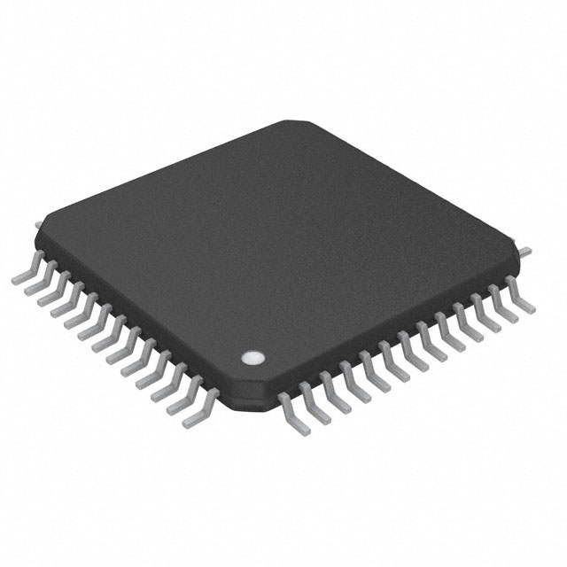
Package: The HI-3582PQI-10 comes in a compact and durable package, ensuring protection during transportation and handling.
Essence: This ADC is designed to provide reliable and accurate conversion of analog signals into digital form, facilitating precise measurements in various applications.
Packaging/Quantity: The HI-3582PQI-10 is typically packaged in reels or trays, with quantities varying based on customer requirements.
Specifications
- Resolution: 16 bits
- Input Voltage Range: ±10V
- Conversion Speed: 1 MSPS (Mega Samples Per Second)
- Power Supply: +5V
- Operating Temperature Range: -40°C to +85°C
- Package Type: QFN (Quad Flat No-Lead)
- Pin Count: 32
Detailed Pin Configuration
The HI-3582PQI-10 has a total of 32 pins, each serving a specific function. Here is a detailed pin configuration:
- VREF-: Negative reference voltage input
- VREF+: Positive reference voltage input
- AGND: Analog ground
- VIN: Analog input voltage
- CLK: Clock input
- CS: Chip select input
- DOUT: Digital output data
- DGND: Digital ground
- DVDD: Digital power supply
- AVDD: Analog power supply
- REFOUT: Reference voltage output
- REFBUF: Reference buffer enable
- PDWN: Power-down control
- SDO: Serial data output
- SDI: Serial data input
- SCLK: Serial clock input 17-32. NC: No connection
Functional Features
The HI-3582PQI-10 offers several functional features that enhance its performance and usability:
- High-resolution conversion: The 16-bit resolution ensures accurate representation of analog signals, enabling precise measurements.
- Low noise performance: The ADC's low noise characteristics minimize signal distortion, resulting in more reliable data acquisition.
- Fast conversion speed: With a conversion speed of 1 MSPS, the HI-3582PQI-10 enables real-time data capture for time-sensitive applications.
- Flexible power supply: The device operates on a +5V power supply, making it compatible with various systems.
- Easy integration: The QFN package and well-defined pin configuration simplify the integration process into existing designs.
Advantages and Disadvantages
Advantages: - High resolution for accurate measurements - Low noise performance for reliable data acquisition - Fast conversion speed for real-time applications - Wide input voltage range for versatile usage - Compact and durable package for protection during handling
Disadvantages: - Limited pin count may restrict certain complex applications - Requires external clock source for operation
Working Principles
The HI-3582PQI-10 operates based on the successive approximation register (SAR) ADC architecture. It utilizes a capacitor array and a comparator to perform the analog-to-digital conversion process. The input voltage is sampled, held, and compared against a reference voltage in a step-by-step manner until the digital representation is obtained.
Detailed Application Field Plans
The HI-3582PQI-10 finds applications in various fields that require precise analog-to-digital conversion. Some of the detailed application field plans include:
- Industrial automation: The ADC can be used for accurate measurement and control in industrial processes, such as temperature sensing, pressure monitoring, and motor control.
- Scientific research: In scientific experiments and data acquisition systems, the HI-3582PQI-10 enables high-resolution measurements of physical quantities, such as voltage, current, and strain.
- Medical equipment: The device can be integrated into medical devices for precise measurement of vital signs, bioelectric signals, and other physiological parameters.
- Test and measurement instruments: The ADC's high resolution and low noise performance make it suitable for
Senaraikan 10 soalan dan jawapan biasa yang berkaitan dengan aplikasi HI-3582PQI-10 dalam penyelesaian teknikal
Sure! Here are 10 common questions and answers related to the application of HI-3582PQI-10 in technical solutions:
1. What is HI-3582PQI-10? HI-3582PQI-10 is a high-performance integrated circuit (IC) designed for use in technical solutions, specifically in industrial automation and control systems.
2. What are the key features of HI-3582PQI-10? Some key features of HI-3582PQI-10 include multiple digital I/O channels, high-speed data transfer capabilities, low power consumption, and compatibility with various communication protocols.
3. Which communication protocols does HI-3582PQI-10 support? HI-3582PQI-10 supports popular communication protocols such as Modbus, Profibus, CAN, and Ethernet/IP, making it versatile for integration into different systems.
4. What are the typical applications of HI-3582PQI-10? HI-3582PQI-10 is commonly used in applications like factory automation, process control, robotics, building management systems, and other industrial control systems.
5. How many digital I/O channels does HI-3582PQI-10 have? HI-3582PQI-10 typically has 16 digital I/O channels, which can be configured as inputs or outputs based on the system requirements.
6. What is the maximum data transfer rate supported by HI-3582PQI-10? HI-3582PQI-10 supports high-speed data transfer rates up to 1 Mbps, ensuring efficient communication between devices in the system.
7. Is HI-3582PQI-10 compatible with both 3.3V and 5V logic levels? Yes, HI-3582PQI-10 is designed to be compatible with both 3.3V and 5V logic levels, providing flexibility in system design and integration.
8. Does HI-3582PQI-10 have built-in protection features? Yes, HI-3582PQI-10 incorporates built-in protection features such as overvoltage protection, short-circuit protection, and thermal shutdown to ensure the safety and reliability of the system.
9. Can HI-3582PQI-10 operate in harsh industrial environments? Yes, HI-3582PQI-10 is designed to operate reliably in harsh industrial environments, with a wide operating temperature range and robust construction to withstand vibrations and shocks.
10. Is there any software development kit (SDK) available for HI-3582PQI-10? Yes, the manufacturer provides a comprehensive software development kit (SDK) that includes libraries, drivers, and example codes to facilitate the integration and programming of HI-3582PQI-10 into technical solutions.
Please note that the specific details and answers may vary depending on the manufacturer's documentation and specifications of HI-3582PQI-10.