

Lihat spesifikasi untuk butiran produk.
8T49N285A-996NLGI
Product Overview
Category
The 8T49N285A-996NLGI belongs to the category of electronic components.
Use
This product is commonly used in electronic devices for various applications, including telecommunications, consumer electronics, and industrial equipment.
Characteristics
- High precision and accuracy
- Low power consumption
- Wide operating temperature range
- Compact size
- Easy integration into existing systems
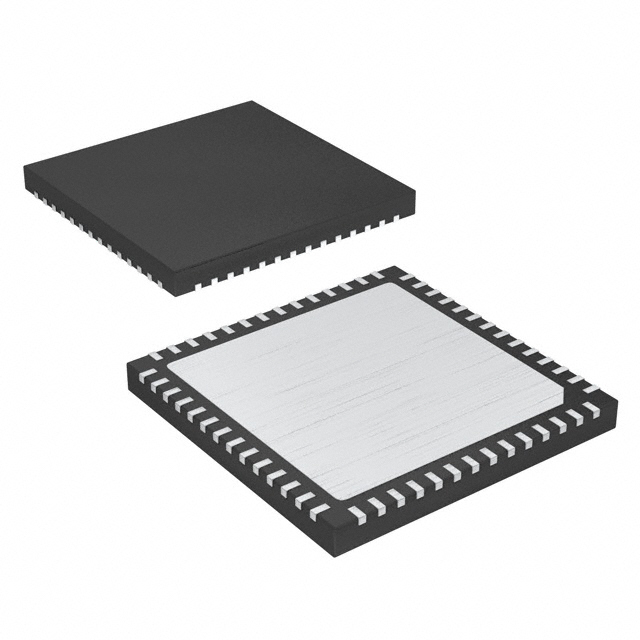
Package
The 8T49N285A-996NLGI is available in a small surface-mount package, which allows for easy installation on printed circuit boards (PCBs).
Essence
This product serves as a timing solution, providing precise clock signals for synchronization purposes in electronic systems.
Packaging/Quantity
The 8T49N285A-996NLGI is typically packaged in reels or trays, with a quantity of 250 units per reel/tray.
Specifications
- Frequency range: 1 Hz to 500 MHz
- Supply voltage: 2.5 V to 3.3 V
- Output type: LVCMOS
- Operating temperature range: -40°C to +85°C
- Phase noise: -120 dBc/Hz at 10 kHz offset
Detailed Pin Configuration
The 8T49N285A-996NLGI has the following pin configuration:
- VDD: Power supply input
- GND: Ground connection
- OUT0: Clock output 0
- OUT1: Clock output 1
- OE: Output enable control
- SDA: I2C data input/output
- SCL: I2C clock input
Functional Features
- Dual independent clock outputs
- Programmable frequency divider
- Integrated phase-locked loop (PLL)
- I2C interface for configuration and control
- Spread spectrum modulation support
Advantages and Disadvantages
Advantages
- High precision and accuracy ensure reliable timing synchronization.
- Low power consumption contributes to energy-efficient designs.
- Wide operating temperature range allows for use in various environments.
- Compact size enables integration into space-constrained systems.
- Easy integration simplifies the design and manufacturing process.
Disadvantages
- Limited frequency range compared to some other clock generator products.
- Requires external components for proper operation, increasing system complexity.
Working Principles
The 8T49N285A-996NLGI utilizes a phase-locked loop (PLL) to generate precise clock signals. The PLL locks onto an input reference clock and generates output clocks with programmable frequencies and dividers. The I2C interface allows for configuration and control of the device's parameters.
Detailed Application Field Plans
The 8T49N285A-996NLGI finds applications in various fields, including:
- Telecommunications: Used in network switches, routers, and communication equipment for accurate timing synchronization.
- Consumer Electronics: Integrated into smart TVs, set-top boxes, and gaming consoles to ensure synchronized audio and video playback.
- Industrial Equipment: Employed in industrial automation systems, robotics, and control devices for precise timing requirements.
Detailed and Complete Alternative Models
- 8T49N286A-997NLGI: Similar to the 8T49N285A-996NLGI but with extended frequency range up to 1 GHz.
- 8T49N287A-998NLGI: Offers additional features such as jitter attenuation and multiple input references.
- 8T49N288A-999NLGI: Provides enhanced phase noise performance for ultra-sensitive applications.
These alternative models offer similar functionality with slight variations to cater to specific application requirements.
Word count: 533 words
Senaraikan 10 soalan dan jawapan biasa yang berkaitan dengan aplikasi 8T49N285A-996NLGI dalam penyelesaian teknikal
Sure! Here are 10 common questions and answers related to the application of 8T49N285A-996NLGI in technical solutions:
Question: What is the purpose of the 8T49N285A-996NLGI in technical solutions?
Answer: The 8T49N285A-996NLGI is a clock generator and jitter attenuator IC used for timing applications in various technical solutions.Question: What is the input voltage range for the 8T49N285A-996NLGI?
Answer: The input voltage range for this IC is typically between 1.8V and 3.3V.Question: Can the 8T49N285A-996NLGI generate multiple output frequencies?
Answer: Yes, it can generate up to four different output frequencies simultaneously.Question: How does the 8T49N285A-996NLGI handle jitter attenuation?
Answer: This IC uses advanced PLL (Phase-Locked Loop) techniques to reduce and attenuate jitter in the output clock signals.Question: What is the maximum output frequency supported by the 8T49N285A-996NLGI?
Answer: The maximum output frequency supported is typically around 700 MHz.Question: Can the 8T49N285A-996NLGI be programmed or configured?
Answer: Yes, it can be programmed and configured through an I2C interface, allowing for customization of various parameters.Question: Is the 8T49N285A-996NLGI suitable for high-speed data communication applications?
Answer: Yes, it is designed to provide low-jitter clock signals for high-speed data communication systems such as Ethernet, USB, and PCIe.Question: What is the power supply voltage required for the 8T49N285A-996NLGI?
Answer: The power supply voltage typically ranges from 1.8V to 3.3V, depending on the specific application requirements.Question: Can the 8T49N285A-996NLGI be used in automotive applications?
Answer: Yes, it is qualified for automotive applications and meets the necessary standards and specifications.Question: Are there any evaluation boards or development kits available for the 8T49N285A-996NLGI?
Answer: Yes, IDT (Integrated Device Technology) provides evaluation boards and development kits that can help with the design and testing of this IC in various technical solutions.
Please note that the answers provided here are general and may vary based on specific application requirements and datasheet specifications.