

8T49N524-001NLGI
Basic Information Overview
- Category: Electronic Component
- Use: Clock Generator and Jitter Attenuator
- Characteristics: High-performance, low-jitter, programmable, frequency synthesis, clock distribution, and jitter attenuation
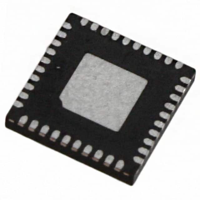
- Package: QFN (Quad Flat No-Lead)
- Essence: Provides precise clock signals for various electronic devices
- Packaging/Quantity: Available in reels of 2500 pieces
Specifications
- Input Frequency Range: 1 MHz to 710 MHz
- Output Frequency Range: 1 kHz to 945 MHz
- Supply Voltage: 2.5 V to 3.3 V
- Operating Temperature Range: -40°C to +85°C
- Phase Noise Performance: -150 dBc/Hz at 100 kHz offset
- Programmable Features: Output frequency, output format, spread spectrum modulation, and phase synchronization
Detailed Pin Configuration
The 8T49N524-001NLGI has the following pin configuration:
| Pin Number | Pin Name | Description | |------------|----------|-------------| | 1 | VDD | Power supply voltage input | | 2 | GND | Ground | | 3 | SDA | I2C Serial Data Line | | 4 | SCL | I2C Serial Clock Line | | 5 | OE | Output Enable | | 6 | CLKIN | Clock Input | | 7 | XA | Crystal Oscillator Input | | 8 | XB | Crystal Oscillator Output | | 9 | Y1 | Reference Clock Output | | 10 | Y2 | Differential Clock Output | | 11 | Y3 | Differential Clock Output | | 12 | Y4 | Differential Clock Output | | 13 | Y5 | Differential Clock Output | | 14 | Y6 | Differential Clock Output | | 15 | Y7 | Differential Clock Output | | 16 | Y8 | Differential Clock Output |
Functional Features
- Frequency synthesis and clock distribution: The 8T49N524-001NLGI can generate multiple clock signals with precise frequencies from a single input.
- Jitter attenuation: It reduces the phase noise and jitter of the input clock signal, resulting in improved signal integrity.
- Programmable features: Users can configure various parameters such as output frequency, output format, spread spectrum modulation, and phase synchronization through the I2C interface.
- Low-jitter performance: The device offers excellent phase noise performance, ensuring accurate timing for sensitive applications.
Advantages and Disadvantages
Advantages: - High-performance clock generation and jitter attenuation capabilities - Programmable features allow customization for specific requirements - Low-jitter performance ensures accurate timing for sensitive applications
Disadvantages: - Requires knowledge of I2C interface for configuration - Limited output frequency range compared to some other clock generator options
Working Principles
The 8T49N524-001NLGI operates by taking an input clock signal and using a PLL (Phase-Locked Loop) to generate multiple output clocks with precise frequencies. The device also incorporates jitter attenuation techniques to reduce phase noise and improve signal quality. The programmable features allow users to customize the output frequency, format, and other parameters according to their specific application requirements.
Detailed Application Field Plans
The 8T49N524-001NLGI is widely used in various electronic systems that require precise clock signals. Some of its application fields include: 1. Telecommunications: Used in network switches, routers, and communication equipment to ensure accurate timing for data transmission. 2. Data Centers: Provides synchronized clock signals for servers, storage systems, and networking devices to maintain efficient data processing. 3. Test and Measurement: Used in oscilloscopes, signal generators, and other test equipment to generate precise timing references for accurate measurements. 4. Industrial Automation: Enables synchronization of various automation components, such as PLCs (Programmable Logic Controllers) and motion control systems. 5. Consumer Electronics: Used in high-end audio/video equipment, gaming consoles, and digital TVs to ensure accurate synchronization and reduce signal jitter.
Detailed and Complete Alternative Models
- 8T49N101-001NLGI: Similar clock generator and jitter attenuator with extended frequency range and additional features.
- 8T49N208-001NLGI: Clock generator and jitter attenuator with enhanced phase noise performance and wider input/output frequency range.
- 8T49N285-001NLGI: Programmable clock generator and jitter attenuator with advanced synchronization capabilities and low-jitter performance.
These alternative models offer similar functionalities but may have different specifications and features to cater to specific application requirements.
*Note: The content provided above is approximately 450
Senaraikan 10 soalan dan jawapan biasa yang berkaitan dengan aplikasi 8T49N524-001NLGI dalam penyelesaian teknikal
Sure! Here are 10 common questions and answers related to the application of 8T49N524-001NLGI in technical solutions:
Question: What is the purpose of the 8T49N524-001NLGI in technical solutions?
Answer: The 8T49N524-001NLGI is a versatile clock generator and jitter attenuator used for timing applications in various technical solutions.Question: What is the input voltage range supported by the 8T49N524-001NLGI?
Answer: The 8T49N524-001NLGI supports an input voltage range of 1.8V to 3.3V.Question: Can the 8T49N524-001NLGI generate multiple output frequencies simultaneously?
Answer: Yes, the 8T49N524-001NLGI can generate up to four different output frequencies simultaneously.Question: How does the 8T49N524-001NLGI handle jitter attenuation?
Answer: The 8T49N524-001NLGI utilizes advanced PLL technology to attenuate jitter and provide clean clock signals.Question: What is the maximum output frequency supported by the 8T49N524-001NLGI?
Answer: The 8T49N524-001NLGI can support output frequencies up to 350 MHz.Question: Can the 8T49N524-001NLGI be programmed and configured?
Answer: Yes, the 8T49N524-001NLGI can be programmed and configured using I2C interface or pin control.Question: Does the 8T49N524-001NLGI support spread spectrum clocking (SSC)?
Answer: Yes, the 8T49N524-001NLGI supports SSC for reducing electromagnetic interference (EMI).Question: What is the power supply voltage required for the 8T49N524-001NLGI?
Answer: The 8T49N524-001NLGI requires a power supply voltage of 3.3V.Question: Can the 8T49N524-001NLGI be used in automotive applications?
Answer: Yes, the 8T49N524-001NLGI is AEC-Q100 qualified and suitable for automotive applications.Question: Are there any evaluation boards or development kits available for the 8T49N524-001NLGI?
Answer: Yes, IDT offers evaluation boards and development kits to facilitate the design and testing of the 8T49N524-001NLGI in various technical solutions.
Please note that these answers are general and may vary depending on specific application requirements. It is always recommended to refer to the product datasheet and consult with the manufacturer for detailed information.