

IDT5V9885BPFGI
Product Overview
Category
The IDT5V9885BPFGI belongs to the category of integrated circuits (ICs).
Use
This product is commonly used in electronic devices for signal switching and routing applications.
Characteristics
- The IDT5V9885BPFGI is a high-performance, low-voltage, bidirectional level translator.
- It operates at a voltage range of 1.2V to 3.6V, making it suitable for various digital systems.
- This IC provides seamless translation between different voltage levels, ensuring compatibility between devices with varying voltage requirements.
Package
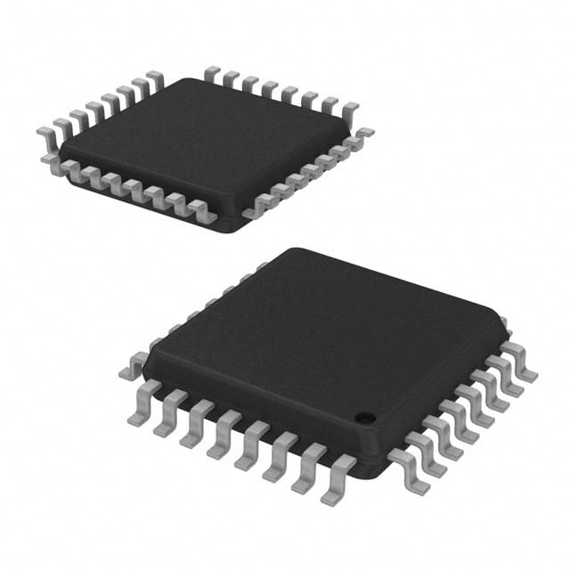
The IDT5V9885BPFGI is available in a small form factor package, such as a 20-pin TSSOP (Thin Shrink Small Outline Package).
Essence
The essence of this product lies in its ability to facilitate communication between devices operating at different voltage levels, enabling smooth data transfer.
Packaging/Quantity
The IDT5V9885BPFGI is typically packaged in reels or tubes, containing a quantity of 250 units per package.
Specifications
- Voltage Range: 1.2V to 3.6V
- Number of Channels: 8
- Input/Output Compatibility: CMOS/TTL
- Operating Temperature Range: -40°C to +85°C
- Supply Current: 10μA (typical)
- Propagation Delay: 4ns (typical)
Detailed Pin Configuration
The IDT5V9885BPFGI features the following pin configuration:
- VCCA - Power supply for side A
- VCCB - Power supply for side B
- GND - Ground
- OE - Output Enable
- A1 - Channel A control input
- A2 - Channel A control input
- A3 - Channel A control input
- A4 - Channel A control input
- B1 - Channel B control input
- B2 - Channel B control input
- B3 - Channel B control input
- B4 - Channel B control input
- I/O1A - Channel A bidirectional data I/O
- I/O2A - Channel A bidirectional data I/O
- I/O3A - Channel A bidirectional data I/O
- I/O4A - Channel A bidirectional data I/O
- I/O1B - Channel B bidirectional data I/O
- I/O2B - Channel B bidirectional data I/O
- I/O3B - Channel B bidirectional data I/O
- I/O4B - Channel B bidirectional data I/O
Functional Features
- Bidirectional voltage level translation between two different voltage domains.
- Automatic direction sensing and control for seamless data transfer.
- Low power consumption, making it suitable for battery-powered devices.
- High-speed operation with minimal propagation delay.
- ESD protection on all pins for enhanced reliability.
Advantages and Disadvantages
Advantages
- Enables communication between devices operating at different voltage levels.
- Easy integration into various digital systems.
- Provides automatic direction sensing, simplifying system design.
- Offers high-speed operation with low propagation delay.
Disadvantages
- Limited to a maximum of 8 channels.
- Requires careful consideration of voltage compatibility to avoid damage to connected devices.
Working Principles
The IDT5V9885BPFGI utilizes a combination of level-shifting circuitry and direction control logic to facilitate bidirectional voltage translation. The device automatically detects the direction of data flow and adjusts the voltage levels accordingly, ensuring seamless communication between devices with different voltage requirements.
Detailed Application Field Plans
The IDT5V9885BPFGI finds applications in various fields, including:
- Consumer Electronics: Used in smartphones, tablets, and gaming consoles for voltage level translation between different components.
- Industrial Automation: Enables communication between devices operating at different voltage levels in control systems and sensors.
- Automotive Electronics: Facilitates data transfer between components with varying voltage requirements in automotive applications.
- Telecommunications: Used in networking equipment to ensure compatibility between devices with different voltage levels.
Detailed and Complete Alternative Models
- Texas Instruments SN74LVCH245APW - 8-bit bidirectional voltage level translator.
- NXP PCA9306DCUR - Dual bidirectional I2C-bus and SMBus voltage level translator.
- ON Semiconductor NC7SZ125P5X - Single bidirectional buffer with voltage level translation.
These alternative models offer similar functionality and can be considered as alternatives to the IDT5V9885BPFGI based on specific application requirements.
Word count: 610 words
Senaraikan 10 soalan dan jawapan biasa yang berkaitan dengan aplikasi IDT5V9885BPFGI dalam penyelesaian teknikal
Sure! Here are 10 common questions and answers related to the application of IDT5V9885BPFGI in technical solutions:
Q: What is the IDT5V9885BPFGI? A: The IDT5V9885BPFGI is a high-performance clock generator and fanout buffer designed for use in various technical solutions.
Q: What are the key features of the IDT5V9885BPFGI? A: The key features include multiple outputs, low jitter, programmable output frequencies, and support for various input clock types.
Q: What applications can benefit from using the IDT5V9885BPFGI? A: The IDT5V9885BPFGI is commonly used in networking equipment, servers, storage systems, and other electronic devices that require precise clock synchronization.
Q: How many outputs does the IDT5V9885BPFGI support? A: The IDT5V9885BPFGI supports up to 12 differential or single-ended outputs.
Q: Can I program the output frequencies of the IDT5V9885BPFGI? A: Yes, the IDT5V9885BPFGI offers flexible frequency programming options to meet specific system requirements.
Q: What types of input clocks does the IDT5V9885BPFGI accept? A: The IDT5V9885BPFGI accepts various input clock types, including LVCMOS, LVDS, HCSL, and SSTL.
Q: Does the IDT5V9885BPFGI provide any clock redundancy features? A: Yes, the IDT5V9885BPFGI supports clock redundancy through its built-in failover and holdover mechanisms.
Q: What is the typical jitter performance of the IDT5V9885BPFGI? A: The IDT5V9885BPFGI offers low jitter performance, typically in the range of a few picoseconds.
Q: Can I control the IDT5V9885BPFGI using an external microcontroller or FPGA? A: Yes, the IDT5V9885BPFGI provides various control interfaces, including I2C, SMBus, and SPI, allowing easy integration with external controllers.
Q: Is the IDT5V9885BPFGI available in different package options? A: Yes, the IDT5V9885BPFGI is available in different package options, such as TSSOP and VFQFPN, to accommodate different PCB layouts and space constraints.
Please note that the answers provided here are general and may vary depending on the specific implementation and requirements of your technical solution.