

QS3384PAG8
Product Overview
- Category: Integrated Circuit
- Use: Digital Switch
- Characteristics: High-speed, Low-power, Bidirectional
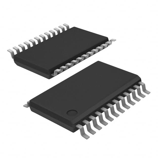
- Package: 20-pin TSSOP (Thin Shrink Small Outline Package)
- Essence: CMOS (Complementary Metal-Oxide-Semiconductor) technology
- Packaging/Quantity: Tape and Reel, 2500 units per reel
Specifications
- Supply Voltage: 2.3V to 3.6V
- Operating Temperature: -40°C to +85°C
- Switching Frequency: Up to 100MHz
- Number of Channels: 10 channels
- Input/Output Type: Single-ended or Differential
- On-Resistance: 5Ω maximum
- Propagation Delay: 1.5ns typical
- Control Interface: Parallel
Detailed Pin Configuration
The QS3384PAG8 has a total of 20 pins. The pin configuration is as follows:
- A1: Channel 1 Input/Output
- B1: Channel 1 Output/Input
- A2: Channel 2 Input/Output
- B2: Channel 2 Output/Input
- A3: Channel 3 Input/Output
- B3: Channel 3 Output/Input
- A4: Channel 4 Input/Output
- B4: Channel 4 Output/Input
- A5: Channel 5 Input/Output
- B5: Channel 5 Output/Input
- GND: Ground
- VCC: Supply Voltage
- OE: Output Enable
- A6: Channel 6 Input/Output
- B6: Channel 6 Output/Input
- A7: Channel 7 Input/Output
- B7: Channel 7 Output/Input
- A8: Channel 8 Input/Output
- B8: Channel 8 Output/Input
- GND: Ground
Functional Features
- Bidirectional digital switch for high-speed data transmission.
- Low power consumption, suitable for battery-powered devices.
- Can be used with single-ended or differential signals.
- Wide operating voltage range allows compatibility with various systems.
- Fast switching frequency enables real-time data processing.
- Parallel control interface simplifies integration into existing designs.
Advantages and Disadvantages
Advantages: - High-speed operation for efficient data transfer. - Low power consumption extends battery life. - Versatile input/output options for flexibility in system design. - Compact package size saves board space. - Easy integration with parallel control interface.
Disadvantages: - Limited number of channels (10 channels). - On-resistance may affect signal integrity in certain applications. - Not suitable for high-voltage applications.
Working Principles
The QS3384PAG8 is based on CMOS technology, which utilizes both NMOS and PMOS transistors to achieve bidirectional signal transmission. When the control signal is activated, the corresponding channel connects the input to the output, allowing data to pass through. The low on-resistance ensures minimal signal attenuation. The device operates within a specified voltage range and can handle high-speed data transmission due to its fast switching characteristics.
Detailed Application Field Plans
The QS3384PAG8 is commonly used in various applications, including:
- Data communication systems
- Networking equipment
- Industrial automation
- Test and measurement instruments
- Consumer electronics
- Automotive electronics
- Medical devices
- Aerospace and defense systems
Detailed and Complete Alternative Models
- SN74CBT3257: 32-channel digital switch with similar characteristics and package.
- MAX3384: 8-channel digital switch with enhanced ESD protection.
- CD74HC4067: 16-channel analog/digital multiplexer with similar package.
These alternative models offer similar functionality and can be considered as substitutes for the QS3384PAG8 in various applications.
Word count: 511 words
Senaraikan 10 soalan dan jawapan biasa yang berkaitan dengan aplikasi QS3384PAG8 dalam penyelesaian teknikal
Sure! Here are 10 common questions and answers related to the application of QS3384PAG8 in technical solutions:
Q: What is QS3384PAG8? A: QS3384PAG8 is a high-performance, low-voltage, bidirectional, dual-supply translating switch with 10-bit voltage level translation capability.
Q: What are the key features of QS3384PAG8? A: The key features include low on-resistance, wide voltage range, bidirectional level shifting, and compatibility with various logic families.
Q: What is the typical application of QS3384PAG8? A: QS3384PAG8 is commonly used for voltage level translation between different logic families, such as TTL to CMOS or CMOS to LVDS.
Q: What is the maximum voltage rating of QS3384PAG8? A: The maximum voltage rating is typically around 5.5V.
Q: Can QS3384PAG8 be used in both unidirectional and bidirectional applications? A: Yes, QS3384PAG8 can be used in both unidirectional and bidirectional applications.
Q: What is the power supply requirement for QS3384PAG8? A: QS3384PAG8 requires a dual power supply with VCCA and VCCB voltages typically ranging from 2.3V to 5.5V.
Q: Does QS3384PAG8 support hot-swapping capability? A: Yes, QS3384PAG8 supports hot-swapping, allowing for easy insertion and removal of devices without disrupting the system.
Q: What is the operating temperature range of QS3384PAG8? A: The operating temperature range is typically from -40°C to +85°C.
Q: Can QS3384PAG8 handle high-speed data signals? A: Yes, QS3384PAG8 is designed to handle high-speed data signals with minimal propagation delay and skew.
Q: Are there any recommended reference designs or application notes available for QS3384PAG8? A: Yes, the manufacturer of QS3384PAG8 provides reference designs and application notes that can help in implementing the chip in various technical solutions.
Please note that the answers provided here are general and may vary depending on specific datasheet specifications and application requirements.