

IRS23364DJPBF
Product Overview
- Category: Integrated Circuit (IC)
- Use: Motor Drive and Control
- Characteristics:
- High voltage, high-speed power MOSFET and IGBT driver
- Three-phase inverter output stage
- Protection features for overcurrent, undervoltage, and overtemperature
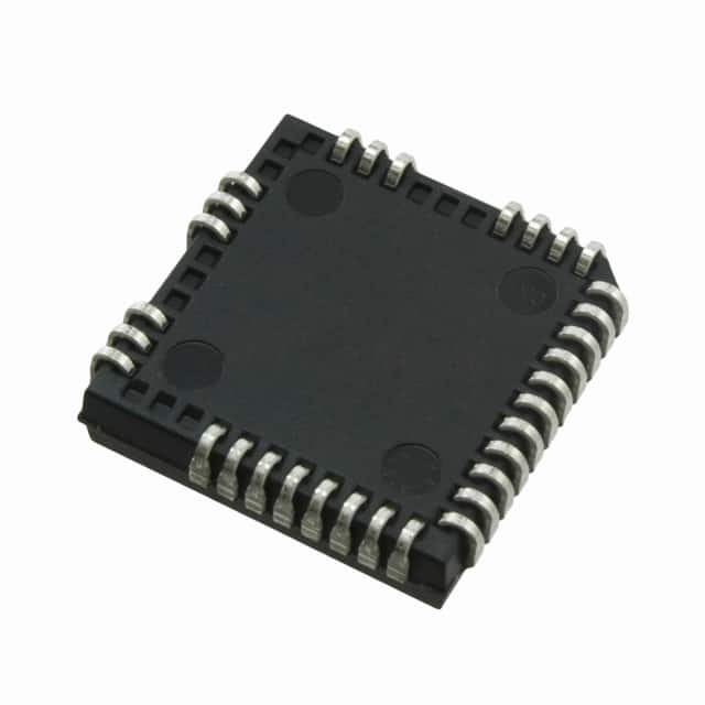
- Package: DIP (Dual In-line Package)
- Essence: Power electronics control and drive IC
- Packaging/Quantity: Available in tubes of 25 units
Specifications
- Operating Voltage Range: 10V to 20V
- Output Current: 1.5A
- Switching Frequency: Up to 500kHz
- Operating Temperature Range: -40°C to +125°C
- Isolation Voltage: 2500Vrms
Detailed Pin Configuration
The IRS23364DJPBF IC has a total of 16 pins arranged as follows:
Pin 1: VCC
   Pin 2: HO1
   Pin 3: LO1
   Pin 4: HO2
   Pin 5: LO2
   Pin 6: HO3
   Pin 7: LO3
   Pin 8: VSS
   Pin 9: SD
   Pin 10: VS
   Pin 11: VB
   Pin 12: NC
   Pin 13: NC
   Pin 14: NC
   Pin 15: NC
   Pin 16: NC
Functional Features
- High voltage level shifting for driving power MOSFETs and IGBTs
- Three-phase inverter output stage with six outputs
- Integrated protection features such as overcurrent, undervoltage, and overtemperature
- Logic inputs compatible with standard CMOS or LSTTL outputs
- Integrated bootstrap diode for high-side gate drive
Advantages and Disadvantages
Advantages: - High voltage capability allows driving of power MOSFETs and IGBTs - Integrated protection features enhance system reliability - Compact DIP package facilitates easy integration into motor control systems - Wide operating temperature range enables use in various environments
Disadvantages: - Limited output current may not be suitable for high-power applications - DIP package may limit thermal dissipation capabilities
Working Principles
The IRS23364DJPBF is designed to control and drive power electronics devices, such as MOSFETs and IGBTs, in motor drive and control applications. It utilizes high voltage level shifting techniques to provide the necessary drive signals for these devices. The integrated three-phase inverter output stage generates the required output waveforms for controlling the motor.
The IC incorporates protection features like overcurrent, undervoltage, and overtemperature, which help safeguard the system from potential faults and failures. Its logic inputs are compatible with standard CMOS or LSTTL outputs, making it easy to interface with microcontrollers or other control circuitry.
Detailed Application Field Plans
The IRS23364DJPBF IC finds application in various motor drive and control systems, including:
- Electric vehicle propulsion systems
- Industrial automation machinery
- HVAC (Heating, Ventilation, and Air Conditioning) systems
- Robotics and mechatronics
- Renewable energy systems (e.g., wind turbines)
Its high voltage capability, compact package, and integrated protection features make it suitable for demanding applications that require efficient and reliable motor control.
Detailed and Complete Alternative Models
- IR2104S: Similar functionality with a different pin configuration
- IRS2336J: Higher output current capability
- IR21844S: Integrated half-bridge driver with additional features
- IRS2453D: Three-phase bridge driver with integrated current sensing
These alternative models offer similar functionalities and can be considered based on specific application requirements.
Word count: 408 words
Senaraikan 10 soalan dan jawapan biasa yang berkaitan dengan aplikasi IRS23364DJPBF dalam penyelesaian teknikal
Sure! Here are 10 common questions and answers related to the application of IRS23364DJPBF in technical solutions:
Q: What is IRS23364DJPBF? A: IRS23364DJPBF is a high-performance three-phase gate driver IC designed for driving power MOSFETs or IGBTs in motor control and power conversion applications.
Q: What is the maximum operating voltage of IRS23364DJPBF? A: The maximum operating voltage of IRS23364DJPBF is 600V.
Q: What is the typical output current capability of IRS23364DJPBF? A: The typical output current capability of IRS23364DJPBF is ±2A.
Q: Can IRS23364DJPBF be used in both low-side and high-side configurations? A: Yes, IRS23364DJPBF can be used in both low-side and high-side configurations.
Q: What is the recommended operating temperature range for IRS23364DJPBF? A: The recommended operating temperature range for IRS23364DJPBF is -40°C to +125°C.
Q: Does IRS23364DJPBF have built-in protection features? A: Yes, IRS23364DJPBF has various built-in protection features such as under-voltage lockout (UVLO), over-current protection (OCP), and thermal shutdown (TSD).
Q: Can IRS23364DJPBF be used in automotive applications? A: Yes, IRS23364DJPBF is qualified for automotive applications and meets the AEC-Q100 standard.
Q: What is the typical propagation delay of IRS23364DJPBF? A: The typical propagation delay of IRS23364DJPBF is 100ns.
Q: Can IRS23364DJPBF be used in high-frequency applications? A: Yes, IRS23364DJPBF can be used in high-frequency applications as it has a fast switching capability.
Q: What is the package type of IRS23364DJPBF? A: IRS23364DJPBF is available in a 28-lead SOIC (Small Outline Integrated Circuit) package.
Please note that these answers are general and may vary depending on the specific application and requirements. It is always recommended to refer to the datasheet and consult with technical experts for detailed information.