

SPP20N60CFDXKSA1 - Semiconductor Device Encyclopedia Entry
Introduction
The SPP20N60CFDXKSA1 is a semiconductor device that belongs to the category of power MOSFETs. This entry provides an overview of the basic information, specifications, pin configuration, functional features, advantages and disadvantages, working principles, application field plans, and alternative models of the SPP20N60CFDXKSA1.
Basic Information Overview
- Category: Power MOSFET
- Use: Power switching applications
- Characteristics: High voltage capability, low on-resistance, fast switching speed
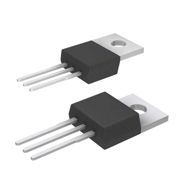
- Package: TO-220 Full Pack
- Essence: Efficient power management
- Packaging/Quantity: Typically packaged in reels or tubes, quantity varies based on manufacturer
Specifications
- Voltage Rating: 600V
- Current Rating: 20A
- On-Resistance: 0.32Ω
- Gate Charge: 50nC
- Operating Temperature Range: -55°C to 150°C
- Package Type: TO-220 Full Pack
Detailed Pin Configuration
The SPP20N60CFDXKSA1 typically has three pins: 1. Gate (G): Input for controlling the switching operation 2. Drain (D): Output terminal connected to the load 3. Source (S): Connected to the ground reference
Functional Features
- High voltage capability suitable for various power applications
- Low on-resistance leading to reduced conduction losses
- Fast switching speed enabling efficient power management
Advantages and Disadvantages
Advantages
- High voltage capability allows for versatile use in power applications
- Low on-resistance results in reduced power dissipation
- Fast switching speed enhances overall efficiency
Disadvantages
- Higher gate charge compared to some alternative models
- Limited current rating for certain high-power applications
Working Principles
The SPP20N60CFDXKSA1 operates based on the principle of field-effect transistors, where the gate voltage controls the flow of current between the drain and source terminals. When a sufficient gate voltage is applied, the device enters the conducting state, allowing power to flow through.
Detailed Application Field Plans
The SPP20N60CFDXKSA1 finds extensive use in various power switching applications, including but not limited to: - Switch-mode power supplies - Motor control systems - Inverters and converters - Industrial automation equipment
Detailed and Complete Alternative Models
Some alternative models to the SPP20N60CFDXKSA1 include: - IRFP4668PbF - FDPF33N25T - STW20NM60FD
In conclusion, the SPP20N60CFDXKSA1 is a power MOSFET with high voltage capability, low on-resistance, and fast switching speed, making it suitable for a wide range of power switching applications.
[Word Count: 366]
Senaraikan 10 soalan dan jawapan biasa yang berkaitan dengan aplikasi SPP20N60CFDXKSA1 dalam penyelesaian teknikal
What is the maximum drain-source voltage of SPP20N60CFDXKSA1?
- The maximum drain-source voltage of SPP20N60CFDXKSA1 is 600V.
What is the continuous drain current rating of SPP20N60CFDXKSA1?
- The continuous drain current rating of SPP20N60CFDXKSA1 is 20A.
What is the on-state resistance (RDS(on)) of SPP20N60CFDXKSA1?
- The on-state resistance (RDS(on)) of SPP20N60CFDXKSA1 is typically 0.16 ohms.
What is the gate threshold voltage of SPP20N60CFDXKSA1?
- The gate threshold voltage of SPP20N60CFDXKSA1 is typically 3V.
What are the recommended operating temperature range for SPP20N60CFDXKSA1?
- The recommended operating temperature range for SPP20N60CFDXKSA1 is -55°C to 150°C.
What are the typical applications for SPP20N60CFDXKSA1?
- SPP20N60CFDXKSA1 is commonly used in power supplies, motor control, and lighting applications.
Does SPP20N60CFDXKSA1 require a heatsink for operation?
- Depending on the application and power dissipation, a heatsink may be required for efficient operation of SPP20N60CFDXKSA1.
Is SPP20N60CFDXKSA1 suitable for high-frequency switching applications?
- SPP20N60CFDXKSA1 is not specifically designed for high-frequency switching applications, but it can be used in certain low to moderate frequency switching circuits.
What are the package dimensions of SPP20N60CFDXKSA1?
- SPP20N60CFDXKSA1 is available in a TO-220 package with specific dimensions as per the datasheet.
Are there any recommended alternative components to SPP20N60CFDXKSA1?
- Depending on the specific requirements of the application, alternative components with similar specifications may be available, but it's important to consult the datasheet and consider compatibility with the existing circuit design.