

5CGXFC9D7F27C8N
Product Overview
Category
The 5CGXFC9D7F27C8N belongs to the category of Field Programmable Gate Arrays (FPGAs).
Use
FPGAs are integrated circuits that can be programmed and reprogrammed to perform various digital functions. The 5CGXFC9D7F27C8N is specifically designed for high-performance applications that require complex logic functions.
Characteristics
- High-performance FPGA with advanced features
- Large capacity for complex designs
- Flexible and reprogrammable
- Low power consumption
- High-speed data processing capabilities
Package
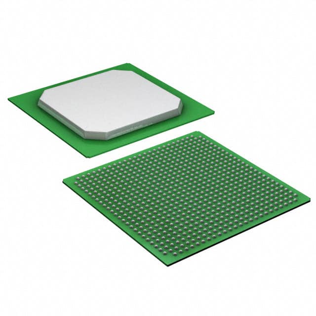
The 5CGXFC9D7F27C8N comes in a compact package, suitable for easy integration into electronic systems. It is available in a surface-mount package.
Essence
The essence of the 5CGXFC9D7F27C8N lies in its ability to provide a customizable and flexible solution for implementing complex digital logic functions.
Packaging/Quantity
The 5CGXFC9D7F27C8N is typically packaged in reels or trays, depending on the manufacturer's specifications. The quantity per package may vary, but it is commonly available in quantities of 100 or more.
Specifications
- Logic Elements: 9,150
- Embedded Memory: 1,638 Kbits
- Maximum User I/Os: 622
- DSP Blocks: 144
- Clock Networks: 12
- Total RAM Bits: 2,621,440
- Operating Voltage: 1.2V
- Operating Temperature: -40°C to 100°C
- Package Type: FBGA
- Package Pins: 780
Detailed Pin Configuration
The 5CGXFC9D7F27C8N has a total of 780 pins, each serving a specific purpose in the FPGA's functionality. The detailed pin configuration can be found in the manufacturer's datasheet.
Functional Features
- High-speed data processing capabilities
- Configurable logic elements for custom designs
- Embedded memory for efficient data storage
- Dedicated DSP blocks for signal processing tasks
- Flexible clock networks for precise timing control
- Support for various communication protocols
- Built-in security features for protecting intellectual property
Advantages and Disadvantages
Advantages
- Flexibility: Can be reprogrammed to adapt to changing requirements.
- High Performance: Capable of handling complex logic functions.
- Low Power Consumption: Helps reduce overall system power consumption.
- Scalability: Can be used in a wide range of applications.
- Cost-Effective: Eliminates the need for custom ASIC development.
Disadvantages
- Complexity: Requires expertise in FPGA programming.
- Limited Resources: The available resources may not be sufficient for extremely large designs.
- Higher Cost: FPGAs can be more expensive compared to other integrated circuits.
Working Principles
The 5CGXFC9D7F27C8N works based on the principle of reconfigurable logic. It consists of an array of configurable logic elements that can be programmed to implement desired digital functions. These logic elements are interconnected through programmable interconnects, allowing for the creation of complex logic circuits. The FPGA can be programmed using hardware description languages (HDL) or graphical tools provided by the manufacturer.
Detailed Application Field Plans
The 5CGXFC9D7F27C8N finds applications in various fields, including:
- Telecommunications: Used in base stations, routers, and network switches for high-speed data processing and protocol handling.
- Aerospace and Defense: Employed in radar systems, avionics, and military communication systems for their high-performance and reconfigurable nature.
- Industrial Automation: Utilized in control systems, robotics, and machine vision applications for real-time data processing and control.
- Medical Devices: Integrated into medical imaging equipment, patient monitoring systems, and diagnostic devices to handle complex algorithms and data processing.
- Automotive: Used in advanced driver-assistance systems (ADAS), infotainment systems, and engine control units (ECUs) for efficient data processing and control.
Detailed and Complete Alternative Models
- 5CGXFC7D6F27C8N
- 5CGXFC9E7F27C8N
- 5CGXFC11D7F27C8N
- 5CGXFC12D7F27C8N
- 5CGXFC15D7F27C8N
These alternative models offer similar features and capabilities to the 5CGXFC9D7F27C8N, but may vary in terms of capacity, I/O count, or other specifications. It is recommended to refer to the
Senaraikan 10 soalan dan jawapan biasa yang berkaitan dengan aplikasi 5CGXFC9D7F27C8N dalam penyelesaian teknikal
Sure! Here are 10 common questions and answers related to the application of 5CGXFC9D7F27C8N in technical solutions:
Q: What is the 5CGXFC9D7F27C8N? A: The 5CGXFC9D7F27C8N is a specific model of Field-Programmable Gate Array (FPGA) manufactured by Intel.
Q: What are the key features of the 5CGXFC9D7F27C8N? A: Some key features of this FPGA include 9,600 Logic Elements, 27,648 Adaptive Look-Up Tables, 1,152 Embedded Multipliers, and support for various I/O standards.
Q: What are the typical applications of the 5CGXFC9D7F27C8N? A: This FPGA can be used in a wide range of applications such as telecommunications, industrial automation, automotive electronics, medical devices, and high-performance computing.
Q: How can I program the 5CGXFC9D7F27C8N? A: You can program this FPGA using Intel's Quartus Prime software, which provides a comprehensive development environment for designing and programming FPGAs.
Q: Can I use the 5CGXFC9D7F27C8N for real-time signal processing? A: Yes, the 5CGXFC9D7F27C8N is capable of handling real-time signal processing tasks due to its high logic capacity and embedded multipliers.
Q: Does the 5CGXFC9D7F27C8N support high-speed serial interfaces? A: Yes, this FPGA supports various high-speed serial interfaces like PCIe, Gigabit Ethernet, and Serial RapidIO, making it suitable for applications requiring fast data transfer.
Q: Can I use the 5CGXFC9D7F27C8N in safety-critical systems? A: Yes, this FPGA is designed to meet industry standards for functional safety, making it suitable for use in safety-critical systems like automotive electronics or medical devices.
Q: What kind of power supply does the 5CGXFC9D7F27C8N require? A: The 5CGXFC9D7F27C8N requires a single 1.2V core voltage supply and multiple auxiliary voltages for different I/O banks.
Q: Can I interface the 5CGXFC9D7F27C8N with external memory devices? A: Yes, this FPGA supports various memory interfaces like DDR3, DDR4, QDR II+, and RLDRAM III, allowing you to interface with external memory devices.
Q: Are there any development boards available for the 5CGXFC9D7F27C8N? A: Yes, Intel provides development kits like the Cyclone V GX Starter Kit, which includes the 5CGXFC9D7F27C8N FPGA, allowing you to quickly prototype and develop your solutions.
Please note that the specific details and answers may vary depending on the context and requirements of your technical solution.