

5SGSMD3H3F35I3L
Product Overview
- Category: Integrated Circuit (IC)
- Use: Digital Signal Processing
- Characteristics: High-performance, Low-power consumption
- Package: BGA (Ball Grid Array)
- Essence: Field Programmable Gate Array (FPGA)
- Packaging/Quantity: Single unit
Specifications
- Manufacturer: Intel Corporation
- Technology: 28nm
- Logic Elements: 220,000
- Embedded Memory: 8,000 Kbits
- Maximum Operating Frequency: 500 MHz
- Operating Voltage: 1.2V
- Temperature Range: -40°C to +100°C
Detailed Pin Configuration
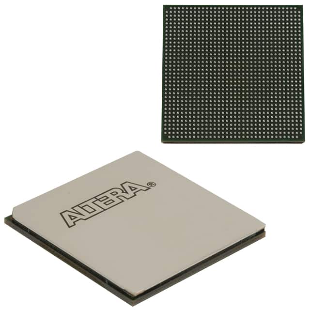
The 5SGSMD3H3F35I3L has a total of 484 pins arranged in a ball grid array package. The pin configuration includes power supply pins, ground pins, input/output pins, clock pins, and configuration pins. Each pin serves a specific purpose and is labeled accordingly.
Functional Features
- High-speed data processing capabilities
- Configurable logic elements for custom designs
- Low-power consumption for energy-efficient applications
- Support for various communication protocols
- On-chip memory for data storage
- Flexible I/O interfaces for connectivity
- Built-in security features for data protection
Advantages and Disadvantages
Advantages
- Versatile and customizable design options
- Faster time-to-market compared to ASICs
- Lower development costs for prototyping
- Reconfigurable for future updates or modifications
- Suitable for a wide range of applications
Disadvantages
- Higher power consumption compared to dedicated hardware
- Limited performance compared to specialized processors
- Complexity in programming and debugging
- Higher cost per unit compared to mass-produced chips
Working Principles
The 5SGSMD3H3F35I3L is based on the Field Programmable Gate Array (FPGA) technology. It consists of a matrix of configurable logic elements and programmable interconnects. The device can be programmed to implement various digital circuits, allowing for flexible and customizable designs. The FPGA's functionality is determined by the configuration data loaded into its internal memory.
Detailed Application Field Plans
The 5SGSMD3H3F35I3L finds applications in various fields, including:
- Telecommunications: Used in base stations, routers, and network switches for high-speed data processing.
- Industrial Automation: Enables control systems, robotics, and machine vision applications.
- Automotive: Utilized in advanced driver-assistance systems (ADAS) and infotainment systems.
- Aerospace: Supports satellite communication, radar systems, and flight control systems.
- Medical Devices: Used in medical imaging, patient monitoring, and laboratory equipment.
Detailed and Complete Alternative Models
- 5SGXEA7N2F45C2LN: Similar FPGA from Intel with higher logic capacity.
- XC7A100T-1FGG484C: FPGA from Xilinx with comparable features and performance.
- LFE5U-85F-8MG285C: FPGA from Lattice Semiconductor with low-power consumption.
These alternative models offer similar functionalities and can be considered as substitutes for the 5SGSMD3H3F35I3L depending on specific requirements.
Word count: 345 words
Senaraikan 10 soalan dan jawapan biasa yang berkaitan dengan aplikasi 5SGSMD3H3F35I3L dalam penyelesaian teknikal
Sure! Here are 10 common questions and answers related to the application of 5SGSMD3H3F35I3L in technical solutions:
Q: What is the 5SGSMD3H3F35I3L FPGA used for? A: The 5SGSMD3H3F35I3L FPGA is commonly used for high-performance applications that require programmable logic and processing capabilities.
Q: What are some typical applications for the 5SGSMD3H3F35I3L FPGA? A: Some typical applications include telecommunications, networking equipment, industrial automation, video processing, and high-speed data acquisition systems.
Q: What are the key features of the 5SGSMD3H3F35I3L FPGA? A: The key features include a high-density programmable logic fabric, embedded memory blocks, high-speed transceivers, and support for various I/O standards.
Q: How does the 5SGSMD3H3F35I3L FPGA handle high-speed data processing? A: The FPGA has dedicated high-speed transceivers that can handle data rates up to several gigabits per second, enabling efficient processing of high-speed data streams.
Q: Can the 5SGSMD3H3F35I3L FPGA be reprogrammed? A: Yes, the FPGA is reprogrammable, allowing users to modify the functionality and behavior of the device as needed.
Q: What development tools are available for programming the 5SGSMD3H3F35I3L FPGA? A: Popular development tools like Quartus Prime from Intel (formerly Altera) are commonly used for programming and configuring the FPGA.
Q: Can the 5SGSMD3H3F35I3L FPGA interface with other components or devices? A: Yes, the FPGA supports various I/O standards and can interface with other components or devices such as memory, sensors, displays, and communication interfaces.
Q: What is the power consumption of the 5SGSMD3H3F35I3L FPGA? A: The power consumption varies depending on the configuration and usage, but it is generally designed to be power-efficient.
Q: Are there any specific design considerations when using the 5SGSMD3H3F35I3L FPGA? A: Yes, some considerations include proper thermal management, signal integrity, power supply requirements, and timing constraints.
Q: Where can I find additional resources and support for the 5SGSMD3H3F35I3L FPGA? A: You can refer to the manufacturer's documentation, online forums, community websites, and technical support channels for additional resources and support.
Please note that the specific details and answers may vary based on the context and requirements of your technical solution.