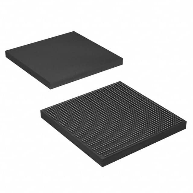
5SGSMD5K3F40C3N
Product Overview
Category
The 5SGSMD5K3F40C3N belongs to the category of Field Programmable Gate Arrays (FPGAs).
Use
This FPGA is primarily used for digital logic applications, such as in telecommunications, automotive, aerospace, and industrial sectors.
Characteristics
- High-performance programmable logic device
- Offers high-speed processing capabilities
- Provides flexibility for custom designs
- Supports complex algorithms and computations
- Enables rapid prototyping and development
Package
The 5SGSMD5K3F40C3N comes in a compact package that ensures easy integration into electronic systems. It is designed to be mounted on printed circuit boards (PCBs) using surface mount technology (SMT).
Essence
The essence of this FPGA lies in its ability to provide reconfigurable hardware that can be programmed to perform specific tasks based on user requirements.
Packaging/Quantity
The 5SGSMD5K3F40C3N is typically packaged in trays or reels, depending on the quantity ordered. The packaging ensures safe transportation and storage of the devices.
Specifications
- Logic Elements: 5,120,000
- Embedded Memory: 10,368 Kbits
- Maximum User I/Os: 1,040
- Clock Management: PLLs and DLLs
- Operating Voltage: 1.2V
- Operating Temperature Range: -40°C to +100°C
- Package Type: F40
- Package Pins: 1517
Detailed Pin Configuration
The detailed pin configuration of the 5SGSMD5K3F40C3N FPGA can be found in the manufacturer's datasheet. It provides information on the pin names, functions, and electrical characteristics.
Functional Features
- High-speed data processing capabilities
- Configurable logic blocks for custom designs
- Dedicated memory blocks for efficient storage
- Built-in clock management units for precise timing control
- Support for various communication protocols
- On-chip debugging and testing features
Advantages and Disadvantages
Advantages
- Flexibility to adapt to changing requirements
- Faster time-to-market for new products
- Reduced development costs compared to custom ASICs
- Ability to reprogram the device for different applications
- High-performance computing capabilities
Disadvantages
- Higher power consumption compared to dedicated hardware
- Limited resources for extremely complex designs
- Steeper learning curve for programming and design implementation
- Higher cost per unit compared to traditional integrated circuits
Working Principles
The 5SGSMD5K3F40C3N FPGA operates based on the principles of configurable logic. It consists of a matrix of programmable logic elements interconnected by configurable routing channels. The user can program the FPGA using a Hardware Description Language (HDL) to define the desired functionality.
During operation, the FPGA's configuration memory is loaded with the user-defined bitstream, which determines the interconnections and behavior of the logic elements. The inputs and outputs of the FPGA are then used to interface with other electronic components in the system.
Detailed Application Field Plans
The 5SGSMD5K3F40C3N FPGA finds extensive application in various fields, including:
- Telecommunications: Used in base stations, network switches, and routers for high-speed data processing and protocol handling.
- Automotive: Employed in advanced driver-assistance systems (ADAS), engine control units (ECUs), and infotainment systems for real-time processing and control.
- Aerospace: Utilized in avionics systems, satellite communication, and radar systems for signal processing and data handling.
- Industrial: Applied in industrial automation, robotics, and control systems for high-performance computing and real-time control.
Detailed and Complete Alternative Models
- 5SGSMD5K2F40C3N: Similar to the 5SGSMD5K3F40C3N but with a lower logic element count.
- 5SGSMD5K4F40C3N: Similar to the 5SGSMD5K3F40C3N but with a higher logic element count.
- 5SGSMD5K3F35C3N: Similar to the 5SGSMD5K3F40C3N but with a different package type.
These alternative models offer varying capabilities and can be chosen based on specific project requirements.
In conclusion, the 5SGSMD5K3F40C3N FPGA is a high-performance programmable logic device that provides flexibility, speed, and versatility for a wide range of digital logic applications. Its advanced features, along with its extensive application field plans, make it a valuable component in various industries.
Senaraikan 10 soalan dan jawapan biasa yang berkaitan dengan aplikasi 5SGSMD5K3F40C3N dalam penyelesaian teknikal
Sure! Here are 10 common questions and answers related to the application of 5SGSMD5K3F40C3N in technical solutions:
Q: What is the 5SGSMD5K3F40C3N FPGA used for? A: The 5SGSMD5K3F40C3N is a Field-Programmable Gate Array (FPGA) that can be used for various applications such as high-performance computing, networking, and signal processing.
Q: What are the key features of the 5SGSMD5K3F40C3N FPGA? A: Some key features include a high logic density, high-speed transceivers, embedded memory blocks, DSP capabilities, and support for various communication protocols.
Q: Can the 5SGSMD5K3F40C3N FPGA be reprogrammed? A: Yes, FPGAs are designed to be reprogrammable, allowing users to modify the functionality of the device even after it has been deployed in a system.
Q: What kind of applications can benefit from using the 5SGSMD5K3F40C3N FPGA? A: Applications that require high-performance processing, real-time data handling, complex algorithms, or custom hardware acceleration can benefit from using this FPGA.
Q: How does the 5SGSMD5K3F40C3N FPGA compare to other FPGAs in its class? A: The 5SGSMD5K3F40C3N offers a good balance between logic density, performance, and power consumption, making it suitable for a wide range of applications.
Q: Does the 5SGSMD5K3F40C3N FPGA support high-speed serial communication? A: Yes, this FPGA has built-in high-speed transceivers that support various protocols such as PCIe, Ethernet, USB, and SATA.
Q: Can the 5SGSMD5K3F40C3N FPGA be used for real-time signal processing? A: Absolutely! With its high logic density and DSP capabilities, this FPGA is well-suited for real-time signal processing applications like image or audio processing.
Q: Are there any development tools available for programming the 5SGSMD5K3F40C3N FPGA? A: Yes, Intel Quartus Prime is a popular software toolchain provided by the manufacturer to program and configure FPGAs, including the 5SGSMD5K3F40C3N.
Q: Can the 5SGSMD5K3F40C3N FPGA interface with other components in a system? A: Yes, this FPGA supports various standard interfaces like GPIO, I2C, SPI, UART, and JTAG, allowing it to communicate with other components in a system.
Q: What kind of power requirements does the 5SGSMD5K3F40C3N FPGA have? A: The power requirements can vary depending on the specific configuration and usage, but typically, this FPGA requires a supply voltage of around 1.0V to 1.2V.
Please note that the answers provided here are general and may vary based on specific implementation details and requirements.


