

5SGXMA3E3H29C2LN
Product Overview
Category
The 5SGXMA3E3H29C2LN belongs to the category of Field Programmable Gate Arrays (FPGAs).
Use
FPGAs are integrated circuits that can be programmed after manufacturing, allowing for flexible and customizable digital logic designs. The 5SGXMA3E3H29C2LN is specifically designed for high-performance applications.
Characteristics
- High-performance FPGA with advanced features
- Large capacity and high-speed processing capabilities
- Flexible and reconfigurable design
- Supports various communication protocols
- Low power consumption
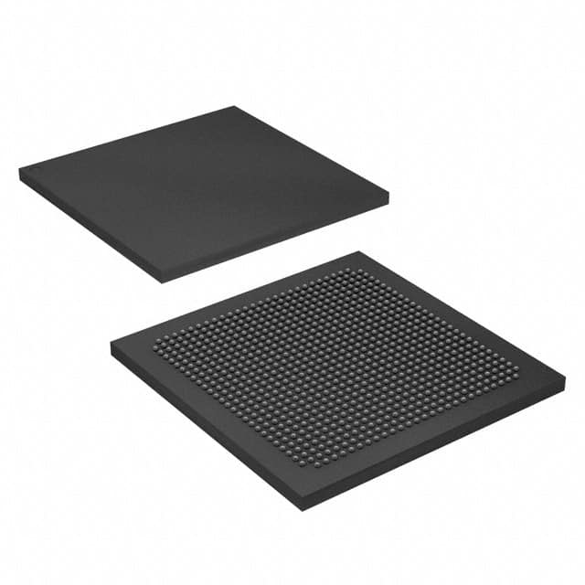
Package
The 5SGXMA3E3H29C2LN comes in a compact and durable package suitable for electronic circuit integration.
Essence
The essence of the 5SGXMA3E3H29C2LN lies in its ability to provide a highly configurable and powerful platform for implementing complex digital systems.
Packaging/Quantity
The 5SGXMA3E3H29C2LN is typically packaged individually and is available in various quantities depending on the customer's requirements.
Specifications
- Logic Elements: 220,000
- Embedded Memory: 8,400 Kbits
- DSP Blocks: 1,288
- Maximum User I/Os: 622
- Transceivers: 24
- Operating Voltage: 1.0V - 1.2V
- Operating Temperature: -40°C to 100°C
- Package Type: F1517
Detailed Pin Configuration
The 5SGXMA3E3H29C2LN has a comprehensive pin configuration, including input/output pins, power supply pins, and configuration pins. For a detailed pin configuration diagram, please refer to the product datasheet.
Functional Features
- High-speed processing capabilities for demanding applications
- Configurable logic elements for flexible design implementation
- Embedded memory blocks for efficient data storage
- DSP blocks for digital signal processing tasks
- Transceivers for high-speed data communication
- Support for various communication protocols (e.g., PCIe, Ethernet)
- Low power consumption for energy-efficient operation
Advantages and Disadvantages
Advantages
- High-performance FPGA suitable for complex designs
- Flexible and reconfigurable platform
- Supports various communication protocols
- Efficient use of embedded memory and DSP blocks
- Low power consumption for energy efficiency
Disadvantages
- Relatively higher cost compared to other programmable logic devices
- Steeper learning curve for programming and design implementation
Working Principles
The 5SGXMA3E3H29C2LN operates based on the principles of configurable logic. It consists of a large number of logic elements that can be interconnected and programmed to perform specific functions. The configuration of these logic elements is stored in non-volatile memory and can be modified as needed. This flexibility allows for the implementation of complex digital systems with high performance.
Detailed Application Field Plans
The 5SGXMA3E3H29C2LN finds applications in various fields, including:
- Telecommunications: Used in network infrastructure equipment, such as routers and switches, for high-speed data processing and communication.
- Aerospace and Defense: Employed in radar systems, avionics, and military communication systems for their high-performance and reconfigurable nature.
- Industrial Automation: Utilized in control systems, robotics, and machine vision applications for real-time processing and control.
- Medical Devices: Integrated into medical imaging systems, patient monitoring devices, and diagnostic equipment for high-speed data processing and analysis.
- Automotive: Applied in advanced driver-assistance systems (ADAS), infotainment systems, and engine control units (ECUs) for enhanced performance and functionality.
Detailed and Complete Alternative Models
- 5SGXEA7K2F40C2N: A similar FPGA model with a larger capacity and more transceivers.
- 5SGXEB6R3F43C2N: Another alternative with lower power consumption and a smaller package size.
- 5SGXEA5H2F35C2N: A cost-effective option with a reduced number of logic elements but still suitable for many applications.
These alternative models offer different combinations of features and specifications to cater to diverse application requirements.
Word count: 560 words
Senaraikan 10 soalan dan jawapan biasa yang berkaitan dengan aplikasi 5SGXMA3E3H29C2LN dalam penyelesaian teknikal
Sure! Here are 10 common questions and answers related to the application of 5SGXMA3E3H29C2LN in technical solutions:
Question: What is the 5SGXMA3E3H29C2LN FPGA used for?
Answer: The 5SGXMA3E3H29C2LN is a Field-Programmable Gate Array (FPGA) that can be used for various applications such as high-performance computing, networking, and signal processing.Question: What is the maximum number of logic elements in the 5SGXMA3E3H29C2LN?
Answer: The 5SGXMA3E3H29C2LN has a maximum of 220,000 logic elements, which allows for complex designs and computations.Question: Can the 5SGXMA3E3H29C2LN support high-speed serial interfaces?
Answer: Yes, the 5SGXMA3E3H29C2LN supports high-speed serial interfaces like PCIe, SATA, and Ethernet, making it suitable for applications requiring fast data transfer.Question: What is the power consumption of the 5SGXMA3E3H29C2LN?
Answer: The power consumption of the 5SGXMA3E3H29C2LN varies depending on the design and usage, but it typically ranges from 10W to 30W.Question: Can the 5SGXMA3E3H29C2LN be reprogrammed?
Answer: Yes, the 5SGXMA3E3H29C2LN is a reprogrammable FPGA, allowing users to modify and update their designs as needed.Question: What development tools are available for programming the 5SGXMA3E3H29C2LN?
Answer: The 5SGXMA3E3H29C2LN can be programmed using Intel Quartus Prime software, which provides a comprehensive development environment for FPGA designs.Question: Does the 5SGXMA3E3H29C2LN have built-in memory?
Answer: No, the 5SGXMA3E3H29C2LN does not have built-in memory. However, it supports external memory interfaces like DDR3 and DDR4 for storing data.Question: Can the 5SGXMA3E3H29C2LN interface with other components or devices?
Answer: Yes, the 5SGXMA3E3H29C2LN has various I/O interfaces such as GPIOs, LVDS, and transceivers, allowing it to interface with other components and devices in a system.Question: What is the operating temperature range of the 5SGXMA3E3H29C2LN?
Answer: The 5SGXMA3E3H29C2LN has an operating temperature range of -40°C to 100°C, making it suitable for both industrial and commercial applications.Question: Are there any reference designs available for the 5SGXMA3E3H29C2LN?
Answer: Yes, Intel provides reference designs and application notes for the 5SGXMA3E3H29C2LN, which can serve as starting points for specific applications and help accelerate development.
Please note that the answers provided here are general and may vary depending on specific use cases and requirements.