

5SGXMA3H2F35C1N
Product Overview
Category
The 5SGXMA3H2F35C1N belongs to the category of Field Programmable Gate Arrays (FPGAs).
Use
This FPGA is designed for high-performance applications that require complex digital logic circuits. It provides a flexible and reconfigurable platform for implementing custom digital designs.
Characteristics
- High-performance FPGA with advanced features
- Large capacity for complex designs
- Reconfigurable architecture allows for flexibility in design modifications
- Low power consumption
- High-speed data processing capabilities
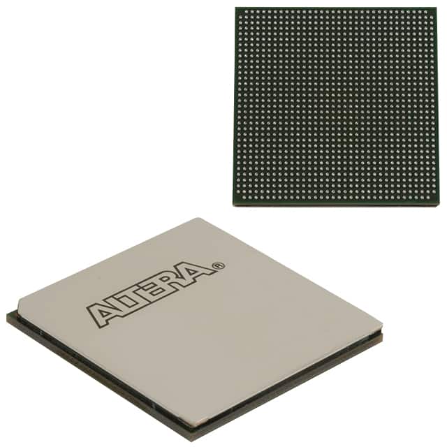
Package
The 5SGXMA3H2F35C1N comes in a compact package suitable for integration into electronic systems. The package ensures protection against environmental factors and facilitates easy installation.
Essence
The essence of the 5SGXMA3H2F35C1N lies in its ability to provide a customizable and high-performance solution for digital circuit design.
Packaging/Quantity
The 5SGXMA3H2F35C1N is typically packaged individually and is available in various quantities depending on the requirements of the user or project.
Specifications
- FPGA Family: Stratix V
- Logic Elements: 220,000
- Embedded Memory: 8,062 Kbits
- DSP Blocks: 1,288
- Maximum User I/Os: 622
- Operating Voltage: 1.0V
- Operating Temperature Range: -40°C to 100°C
- Package Type: F35
- Package Pins: 896
Detailed Pin Configuration
The detailed pin configuration of the 5SGXMA3H2F35C1N can be found in the product datasheet provided by the manufacturer. It includes information about each pin's functionality, voltage levels, and recommended usage.
Functional Features
- High-speed data processing capabilities
- Configurable logic elements for implementing complex digital designs
- Embedded memory blocks for efficient data storage and retrieval
- Dedicated DSP blocks for performing mathematical operations
- Support for various communication protocols
- Flexible clock management resources
- Built-in security features for protecting intellectual property
Advantages and Disadvantages
Advantages
- High-performance FPGA suitable for demanding applications
- Reconfigurable architecture allows for design modifications without hardware changes
- Low power consumption compared to alternative solutions
- Large capacity for implementing complex designs
- Support for various communication protocols enhances compatibility
Disadvantages
- Higher cost compared to other programmable logic devices
- Steeper learning curve for beginners due to the complexity of FPGA programming
- Limited availability of alternative models with similar specifications
Working Principles
The 5SGXMA3H2F35C1N operates based on the principles of reconfigurable computing. It consists of a matrix of configurable logic elements interconnected through programmable routing resources. The user can program the FPGA to implement custom digital circuits by configuring the logic elements and interconnections.
Detailed Application Field Plans
The 5SGXMA3H2F35C1N finds applications in various fields, including: - Telecommunications - Aerospace and defense - Industrial automation - Medical equipment - Data centers - High-performance computing
In telecommunications, it can be used for signal processing, protocol conversion, and network optimization. In aerospace and defense, it can be utilized for radar systems, image processing, and encryption. In industrial automation, it enables control systems and machine vision. In medical equipment, it supports imaging and diagnostics. In data centers and high-performance computing, it provides acceleration for computationally intensive tasks.
Detailed and Complete Alternative Models
While the 5SGXMA3H2F35C1N is a high-performance FPGA, there are alternative models available with similar capabilities. Some of the alternatives include: - Xilinx Virtex UltraScale+ - Intel Stratix 10 - Lattice ECP5 - Microsemi PolarFire
These alternative models offer different features and specifications, allowing users to choose the most suitable FPGA for their specific requirements.
Word count: 550 words
Senaraikan 10 soalan dan jawapan biasa yang berkaitan dengan aplikasi 5SGXMA3H2F35C1N dalam penyelesaian teknikal
Sure! Here are 10 common questions and answers related to the application of 5SGXMA3H2F35C1N in technical solutions:
Q1: What is the 5SGXMA3H2F35C1N? A1: The 5SGXMA3H2F35C1N is a specific model of Field-Programmable Gate Array (FPGA) manufactured by Intel. It offers high-performance capabilities and is commonly used in various technical solutions.
Q2: What are the key features of the 5SGXMA3H2F35C1N? A2: Some key features of the 5SGXMA3H2F35C1N include a large number of logic elements, high-speed transceivers, embedded memory blocks, and support for various communication protocols.
Q3: In what applications can the 5SGXMA3H2F35C1N be used? A3: The 5SGXMA3H2F35C1N can be used in a wide range of applications such as telecommunications, networking, industrial automation, video processing, medical imaging, and high-performance computing.
Q4: How does the 5SGXMA3H2F35C1N differ from other FPGAs? A4: The 5SGXMA3H2F35C1N stands out due to its high logic density, advanced transceiver capabilities, and support for various communication protocols. It offers superior performance and flexibility compared to many other FPGAs.
Q5: Can the 5SGXMA3H2F35C1N be programmed? A5: Yes, the 5SGXMA3H2F35C1N is a field-programmable device, meaning it can be configured and reconfigured to perform specific tasks based on the user's requirements.
Q6: What tools are available for programming the 5SGXMA3H2F35C1N? A6: Intel provides Quartus Prime software, which is commonly used for designing, simulating, and programming FPGAs. It supports the 5SGXMA3H2F35C1N and other Intel FPGA models.
Q7: Can the 5SGXMA3H2F35C1N interface with other components or devices? A7: Yes, the 5SGXMA3H2F35C1N has various I/O interfaces, including high-speed transceivers, LVDS, GPIOs, and memory interfaces, allowing it to communicate with other components or devices in a system.
Q8: What are the power requirements for the 5SGXMA3H2F35C1N? A8: The power requirements for the 5SGXMA3H2F35C1N depend on the specific implementation and configuration. It typically requires multiple power supply voltages, such as core voltage and I/O voltage.
Q9: Are there any development boards available for prototyping with the 5SGXMA3H2F35C1N? A9: Yes, Intel offers development boards like the Arria V GX Starter Kit, which includes the 5SGXMA3H2F35C1N FPGA. These boards provide a platform for prototyping and testing designs.
Q10: Where can I find more information about the 5SGXMA3H2F35C1N? A10: You can find more detailed information about the 5SGXMA3H2F35C1N, including datasheets, user guides, and application notes, on Intel's official website or by contacting their technical support.