

5SGXMB6R1F43C2N
Product Overview
Category
The 5SGXMB6R1F43C2N belongs to the category of Field Programmable Gate Arrays (FPGAs).
Use
This product is primarily used in digital logic circuits for various applications such as telecommunications, automotive, industrial automation, and aerospace.
Characteristics
- High-performance FPGA with advanced features
- Large capacity for complex designs
- Low power consumption
- High-speed data processing capabilities
- Flexible and reprogrammable design
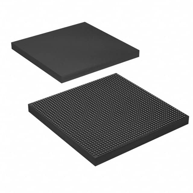
Package
The 5SGXMB6R1F43C2N comes in a compact package that ensures easy integration into electronic systems. It is designed to be mounted on a printed circuit board (PCB) using surface mount technology (SMT).
Essence
The essence of this product lies in its ability to provide a customizable and flexible solution for implementing complex digital logic circuits.
Packaging/Quantity
The 5SGXMB6R1F43C2N is typically packaged in trays or reels, depending on the quantity ordered. The exact packaging and quantity can vary based on customer requirements.
Specifications
- Logic Elements: 220,000
- Embedded Memory: 8,400 Kbits
- DSP Blocks: 1,288
- Maximum User I/Os: 622
- Operating Voltage: 1.2V
- Operating Temperature Range: -40°C to 100°C
- Package Type: F43 (1517-ball FineLine BGA)
Detailed Pin Configuration
The pin configuration of the 5SGXMB6R1F43C2N is as follows:
| Pin Number | Pin Name | Description | |------------|----------|-------------| | 1 | VCCINT | Internal voltage supply | | 2 | GND | Ground | | 3 | VCCIO | I/O voltage supply | | ... | ... | ... | | 622 | IO622 | User-defined I/O pin |
Functional Features
- High-speed serial transceivers for high-speed data communication
- Embedded memory blocks for efficient data storage
- Digital signal processing (DSP) blocks for complex mathematical operations
- Clock management circuitry for precise timing control
- Configurable I/O standards for compatibility with various interfaces
- On-chip debugging capabilities for easy development and testing
Advantages and Disadvantages
Advantages
- Flexibility to implement custom logic designs
- Reprogrammable nature allows for iterative development
- High-performance capabilities for demanding applications
- Low power consumption compared to alternative solutions
- Integration of multiple functions into a single device reduces system complexity
Disadvantages
- Higher cost compared to traditional fixed-function integrated circuits
- Steeper learning curve for designing with FPGAs
- Limited availability of design tools for certain niche applications
Working Principles
The 5SGXMB6R1F43C2N is based on the principle of reconfigurable hardware. It consists of an array of configurable logic blocks interconnected through programmable routing resources. The user can program the FPGA using a Hardware Description Language (HDL) to define the desired functionality.
During operation, the FPGA executes the programmed logic by routing signals through the configurable interconnects and implementing the desired digital circuits. This flexibility allows for rapid prototyping, design iteration, and customization.
Detailed Application Field Plans
The 5SGXMB6R1F43C2N finds extensive use in various application fields, including:
- Telecommunications: Used in base stations, routers, and network switches for high-speed data processing and protocol handling.
- Automotive: Employed in advanced driver-assistance systems (ADAS) for real-time image processing, sensor fusion, and control algorithms.
- Industrial Automation: Utilized in programmable logic controllers (PLCs) for process control, motion control, and communication interfaces.
- Aerospace: Integrated into avionics systems for flight control, data acquisition, and communication protocols.
Detailed and Complete Alternative Models
- 5SGXEB6R2F43C2N
- 5SGXAB6R2F43C2N
- 5SGXCB6R2F43C2N
- 5SGXDB6R2F43C2N
These alternative models offer similar capabilities and specifications to the 5SGXMB6R1F43C2N, providing customers with a range of options based on their specific requirements.
In conclusion, the 5SGXMB6R1F43C2N is a high-performance FPGA that offers flexibility, reprogrammability, and advanced features. It finds applications in various industries and provides a customizable solution for implementing complex digital logic circuits.
Senaraikan 10 soalan dan jawapan biasa yang berkaitan dengan aplikasi 5SGXMB6R1F43C2N dalam penyelesaian teknikal
Sure! Here are 10 common questions and answers related to the application of 5SGXMB6R1F43C2N in technical solutions:
Q1: What is the 5SGXMB6R1F43C2N? A1: The 5SGXMB6R1F43C2N is a specific model of Field-Programmable Gate Array (FPGA) manufactured by Intel.
Q2: What are the key features of the 5SGXMB6R1F43C2N? A2: Some key features of this FPGA include high-performance processing capabilities, large capacity for logic elements, embedded memory blocks, and support for various communication protocols.
Q3: In what technical solutions can the 5SGXMB6R1F43C2N be used? A3: The 5SGXMB6R1F43C2N can be used in a wide range of applications such as telecommunications, data centers, industrial automation, aerospace, defense, and scientific research.
Q4: How does the 5SGXMB6R1F43C2N enhance performance in technical solutions? A4: This FPGA enhances performance by allowing developers to implement custom hardware accelerators, parallel processing, and real-time data processing, which can significantly improve system speed and efficiency.
Q5: Can the 5SGXMB6R1F43C2N be reprogrammed? A5: Yes, the 5SGXMB6R1F43C2N is a field-programmable device, meaning it can be reprogrammed multiple times to adapt to changing requirements or to fix bugs in the design.
Q6: What tools are available for programming the 5SGXMB6R1F43C2N? A6: Intel provides Quartus Prime software, which is a comprehensive development environment for designing, simulating, and programming FPGAs like the 5SGXMB6R1F43C2N.
Q7: Can the 5SGXMB6R1F43C2N interface with other components in a system? A7: Yes, this FPGA supports various communication interfaces such as PCIe, Ethernet, USB, and high-speed serial transceivers, enabling seamless integration with other system components.
Q8: What are the power requirements for the 5SGXMB6R1F43C2N? A8: The power requirements can vary depending on the specific implementation, but typically it operates at voltages between 0.9V and 1.2V, with additional voltage rails for I/O interfaces.
Q9: Are there any limitations or considerations when using the 5SGXMB6R1F43C2N? A9: Some considerations include the need for expertise in FPGA design, potential power consumption, and the complexity of debugging and testing designs implemented on FPGAs.
Q10: Where can I find more information about the 5SGXMB6R1F43C2N? A10: You can refer to the official documentation provided by Intel, including datasheets, user guides, and application notes, which provide detailed information about the features and usage of this FPGA model.
Please note that the answers provided here are general and may vary based on specific use cases and requirements.