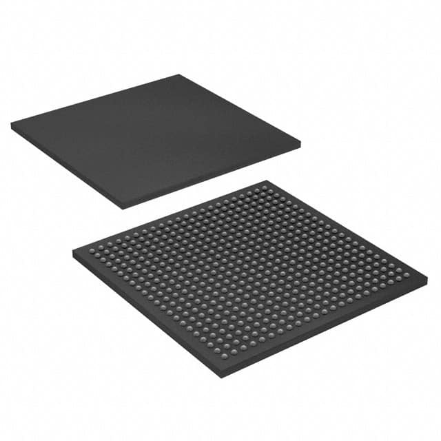
EP1AGX35CF484C6
Product Overview
- Category: Programmable Logic Device (PLD)
- Use: EP1AGX35CF484C6 is a PLD used for digital logic design and implementation.
- Characteristics: It offers high-performance, low-power consumption, and flexibility in designing complex digital circuits.
- Package: The EP1AGX35CF484C6 comes in a 484-pin FineLine BGA package.
- Essence: This PLD provides a versatile platform for implementing various digital logic functions.
- Packaging/Quantity: The EP1AGX35CF484C6 is typically sold individually.
Specifications
- Logic Elements: 33,280
- Embedded Memory: 1,152 Kbits
- User I/O Pins: 346
- Maximum Operating Frequency: 500 MHz
- Supply Voltage: 1.2V
- Operating Temperature Range: -40°C to 100°C
Detailed Pin Configuration
The EP1AGX35CF484C6 has a total of 484 pins. These pins are divided into different categories, including power supply pins, ground pins, configuration pins, input/output pins, and dedicated pins for specific functionalities. A detailed pin configuration diagram can be found in the product datasheet.
Functional Features
- High-density programmable logic device suitable for complex digital designs.
- Offers a wide range of logic elements and embedded memory for efficient implementation.
- Supports various I/O standards for interfacing with external devices.
- Provides advanced clock management features for precise timing control.
- Includes built-in intellectual property (IP) cores for common functions like memory controllers and communication interfaces.
Advantages and Disadvantages
Advantages: - High-performance and low-power consumption. - Flexible and versatile for implementing complex digital circuits. - Extensive library of IP cores available for easy integration. - Supports various I/O standards for compatibility with different devices.
Disadvantages: - Relatively high cost compared to simpler programmable logic devices. - Steeper learning curve for beginners due to its complexity. - Limited availability of alternative models from other manufacturers.
Working Principles
The EP1AGX35CF484C6 is based on the field-programmable gate array (FPGA) technology. It consists of an array of configurable logic blocks interconnected through programmable routing resources. The device can be programmed using hardware description languages (HDLs) or graphical design tools to define the desired digital circuit functionality. Once programmed, the PLD operates by routing signals through the configured logic elements and memory blocks to perform the specified operations.
Detailed Application Field Plans
The EP1AGX35CF484C6 finds applications in various fields, including: - Telecommunications: Used in network routers, switches, and communication equipment. - Industrial Automation: Employed in control systems, robotics, and process automation. - Aerospace and Defense: Utilized in avionics, radar systems, and military-grade electronics. - Automotive: Integrated into automotive electronics for advanced driver assistance systems (ADAS) and infotainment. - Consumer Electronics: Found in high-end audio/video equipment, gaming consoles, and smart home devices.
Detailed and Complete Alternative Models
While the EP1AGX35CF484C6 is a popular choice for many applications, there are alternative models available from other manufacturers. Some notable alternatives include: - Xilinx Virtex-7 series - Intel Cyclone V series - Lattice ECP5 series
These alternative models offer similar capabilities and can be considered based on specific project requirements.
Word count: 315 words
Senaraikan 10 soalan dan jawapan biasa yang berkaitan dengan aplikasi EP1AGX35CF484C6 dalam penyelesaian teknikal
Sure! Here are 10 common questions and answers related to the application of EP1AGX35CF484C6 in technical solutions:
Q1: What is EP1AGX35CF484C6? A1: EP1AGX35CF484C6 is a specific model of field-programmable gate array (FPGA) manufactured by Intel. It offers a range of programmable logic and I/O capabilities for various applications.
Q2: What are the key features of EP1AGX35CF484C6? A2: Some key features of EP1AGX35CF484C6 include 35,000 logic elements, 1,080 Kbits of embedded memory, 4 PLLs, and support for various I/O standards.
Q3: What are the typical applications of EP1AGX35CF484C6? A3: EP1AGX35CF484C6 can be used in a wide range of applications such as industrial automation, telecommunications, automotive systems, medical devices, and high-performance computing.
Q4: How can EP1AGX35CF484C6 be programmed? A4: EP1AGX35CF484C6 can be programmed using hardware description languages (HDLs) like VHDL or Verilog, along with design software provided by Intel, such as Quartus Prime.
Q5: What are the power requirements for EP1AGX35CF484C6? A5: EP1AGX35CF484C6 typically requires a supply voltage of 1.2V for core logic and 3.3V for I/O banks. The power consumption varies depending on the design and operating conditions.
Q6: Can EP1AGX35CF484C6 interface with other components or devices? A6: Yes, EP1AGX35CF484C6 supports various I/O standards, including LVDS, SSTL, and HSTL, allowing it to interface with a wide range of components and devices.
Q7: What tools are available for debugging and testing EP1AGX35CF484C6 designs? A7: Intel provides a suite of design tools, including SignalTap II Logic Analyzer and In-System Memory Content Editor, which can be used for debugging and testing EP1AGX35CF484C6 designs.
Q8: Can EP1AGX35CF484C6 be reprogrammed after deployment? A8: Yes, EP1AGX35CF484C6 is a reprogrammable FPGA, meaning that its configuration can be modified even after it has been deployed in a system.
Q9: Are there any limitations or considerations when using EP1AGX35CF484C6? A9: Some considerations include power consumption, thermal management, and ensuring proper signal integrity due to the high-speed nature of FPGA designs. The datasheet and application notes provide more detailed information.
Q10: Where can I find additional resources and support for EP1AGX35CF484C6? A10: Intel's website offers comprehensive documentation, datasheets, reference designs, and an active community forum where you can find additional resources and support for EP1AGX35CF484C6.
Please note that the answers provided here are general and may vary depending on specific requirements and use cases.


