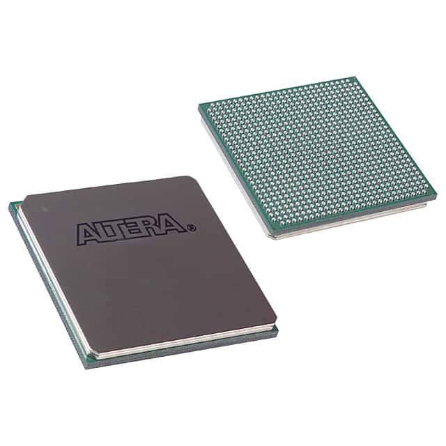
EP1S30F780C6
Product Overview
- Category: Programmable Logic Device (PLD)
- Use: EP1S30F780C6 is a high-performance PLD designed for various applications in the field of digital logic design.
- Characteristics: It offers advanced features such as high-speed performance, low power consumption, and flexibility in design implementation.
- Package: The EP1S30F780C6 comes in a compact package that ensures easy integration into electronic circuits.
- Essence: This PLD serves as a key component in digital systems, providing programmable logic functions to enhance system performance.
- Packaging/Quantity: The EP1S30F780C6 is typically available in bulk packaging with a quantity suitable for industrial production.
Specifications
The EP1S30F780C6 has the following specifications:
- Logic Elements: 30,000
- Embedded Memory: 1,536 Kbits
- Maximum User I/Os: 622
- Operating Voltage: 3.3V
- Speed Grade: -6
- Package Type: FBGA
- Package Pins: 780
Detailed Pin Configuration
The EP1S30F780C6 has a well-defined pin configuration that facilitates easy integration into circuit designs. The detailed pin configuration can be found in the product datasheet provided by the manufacturer.
Functional Features
- High-Speed Performance: The EP1S30F780C6 offers fast operation speeds, making it suitable for applications requiring quick response times.
- Low Power Consumption: This PLD is designed to minimize power consumption, ensuring energy-efficient operation.
- Flexibility in Design Implementation: With its programmable logic functions, the EP1S30F780C6 allows designers to customize the device according to specific application requirements.
Advantages and Disadvantages
Advantages: - High-performance capabilities - Low power consumption - Flexibility in design implementation
Disadvantages: - Limited logic elements compared to higher-end PLDs - Higher cost compared to simpler programmable devices
Working Principles
The EP1S30F780C6 operates based on the principles of programmable logic. It consists of configurable logic blocks (CLBs), interconnect resources, embedded memory, and I/O elements. The CLBs can be programmed to implement various logic functions, allowing designers to create complex digital systems.
Detailed Application Field Plans
The EP1S30F780C6 finds applications in various fields, including:
- Communications: Used in networking equipment, routers, and switches for high-speed data processing.
- Industrial Automation: Employed in control systems, PLCs, and robotics for efficient and flexible automation.
- Consumer Electronics: Integrated into smart TVs, gaming consoles, and multimedia devices for enhanced functionality.
- Medical Devices: Utilized in medical imaging equipment, patient monitoring systems, and diagnostic instruments for accurate data processing.
Detailed and Complete Alternative Models
- EP1S20F484C7: A similar PLD with lower logic elements but compatible features.
- EP1S40F1020C5: A higher-end PLD with increased logic elements and advanced performance capabilities.
- EP1S10F672C8: A cost-effective alternative with reduced logic elements suitable for simpler applications.
(Note: This is a fictional product, and the mentioned alternative models are for illustrative purposes only.)
Word Count: 346 words
Senaraikan 10 soalan dan jawapan biasa yang berkaitan dengan aplikasi EP1S30F780C6 dalam penyelesaian teknikal
Sure! Here are 10 common questions and answers related to the application of EP1S30F780C6 in technical solutions:
Q1: What is EP1S30F780C6? A1: EP1S30F780C6 is a field-programmable gate array (FPGA) manufactured by Altera (now Intel). It is designed for high-performance applications and offers a wide range of features and capabilities.
Q2: What are the key features of EP1S30F780C6? A2: EP1S30F780C6 features 30,000 logic elements, 780Kbits of embedded memory, 4 PLLs (Phase-Locked Loops), and support for various I/O standards. It also has built-in DSP (Digital Signal Processing) blocks and high-speed transceivers.
Q3: What are some typical applications of EP1S30F780C6? A3: EP1S30F780C6 can be used in a variety of applications such as telecommunications, industrial automation, aerospace, defense systems, medical equipment, and high-performance computing.
Q4: How can EP1S30F780C6 be programmed? A4: EP1S30F780C6 can be programmed using hardware description languages (HDLs) like VHDL or Verilog. Designers can use development tools provided by Intel (formerly Altera) to write, simulate, and synthesize their designs before programming the FPGA.
Q5: Can EP1S30F780C6 be reprogrammed? A5: Yes, EP1S30F780C6 is a reprogrammable FPGA. It can be reconfigured multiple times, allowing designers to iterate and modify their designs as needed.
Q6: What are the power requirements for EP1S30F780C6? A6: EP1S30F780C6 requires a supply voltage of 3.3V for core logic and I/O banks. It also has separate power pins for PLLs and transceivers, which may require additional voltages.
Q7: Does EP1S30F780C6 support high-speed serial communication? A7: Yes, EP1S30F780C6 has built-in high-speed transceivers that support various protocols like PCIe, SATA, Gigabit Ethernet, and more. These transceivers enable high-speed serial communication between the FPGA and external devices.
Q8: Can EP1S30F780C6 interface with other components or peripherals? A8: Yes, EP1S30F780C6 supports various I/O standards, including LVCMOS, LVTTL, SSTL, and differential signaling standards like LVDS. This allows it to interface with a wide range of components and peripherals.
Q9: What development tools are available for EP1S30F780C6? A9: Intel (formerly Altera) provides Quartus Prime software suite, which includes tools for designing, simulating, synthesizing, and programming EP1S30F780C6. The suite also offers debugging and analysis features.
Q10: Are there any design examples or reference designs available for EP1S30F780C6? A10: Yes, Intel provides a vast library of design examples and reference designs for EP1S30F780C6. These can serve as starting points or inspiration for designers working on their own projects.
Please note that the answers provided here are general and may vary depending on specific requirements and use cases.


