

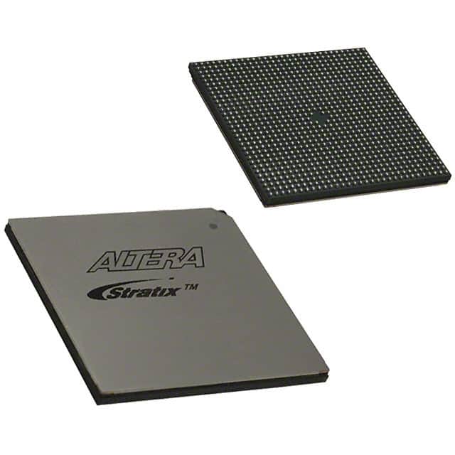
EP1S40B956C6N
Basic Information Overview
- Category: Integrated Circuit (IC)
- Use: Programmable Logic Device (PLD)
- Characteristics: High-performance, low-power consumption
- Package: BGA (Ball Grid Array)
- Essence: Field-Programmable Gate Array (FPGA)
- Packaging/Quantity: Single unit
Specifications
- Model: EP1S40B956C6N
- Technology: 90nm
- Logic Elements: 40,000
- Maximum User I/Os: 956
- Operating Voltage: 1.2V
- Speed Grade: C6
- Temperature Range: -40°C to +85°C
Detailed Pin Configuration
The EP1S40B956C6N has a total of 956 pins, which are divided into various categories: - Power Supply Pins: These pins provide the necessary voltage and ground connections for the device. - Input/Output Pins: These pins are used to interface with external devices and circuits. - Configuration Pins: These pins are used for programming and configuring the FPGA. - Clock Pins: These pins provide clock signals for synchronous operation. - Special Function Pins: These pins have specific functions depending on the application.
Functional Features
- High Performance: The EP1S40B956C6N offers fast processing speeds and efficient logic utilization.
- Low Power Consumption: It is designed to minimize power consumption, making it suitable for battery-powered applications.
- Flexibility: Being a field-programmable device, it allows users to customize the functionality according to their requirements.
- Scalability: The FPGA architecture enables easy integration of additional features and expansion of the design.
- Reliability: The device is built with robust materials and undergoes rigorous testing to ensure reliable operation.
Advantages and Disadvantages
Advantages: - Versatility: The EP1S40B956C6N can be used in a wide range of applications due to its programmable nature. - Cost-Effective: It eliminates the need for custom-designed ASICs, reducing development costs. - Time-to-Market: The FPGA's reprogrammability allows for faster prototyping and shorter development cycles.
Disadvantages: - Complexity: Designing and programming an FPGA requires specialized knowledge and expertise. - Limited Resources: The number of logic elements and I/O pins may restrict the complexity of designs that can be implemented.
Working Principles
The EP1S40B956C6N is based on the principle of configurable logic blocks (CLBs) interconnected through programmable interconnects. These CLBs consist of look-up tables (LUTs), flip-flops, and other components. By configuring the interconnections and programming the LUTs, users can implement desired logic functions and create complex digital circuits.
Detailed Application Field Plans
The EP1S40B956C6N finds applications in various fields, including: - Telecommunications: Used in network routers, switches, and communication equipment. - Industrial Automation: Employed in control systems, robotics, and process automation. - Automotive: Integrated into automotive electronics for engine control, driver assistance systems, and infotainment. - Aerospace: Utilized in avionics, satellite communication, and flight control systems. - Consumer Electronics: Found in high-definition televisions, gaming consoles, and multimedia devices.
Detailed and Complete Alternative Models
- EP1S30F780C5N
- EP2S60F672C5N
- EP3C25F324C8N
- EP4CE115F29C7N
These alternative models offer different specifications and capabilities, allowing users to choose the most suitable option for their specific requirements.
Word count: 457 words
Senaraikan 10 soalan dan jawapan biasa yang berkaitan dengan aplikasi EP1S40B956C6N dalam penyelesaian teknikal
Sure! Here are 10 common questions and answers related to the application of EP1S40B956C6N in technical solutions:
Q1: What is EP1S40B956C6N? A1: EP1S40B956C6N is a specific model of Field-Programmable Gate Array (FPGA) manufactured by Intel.
Q2: What are the key features of EP1S40B956C6N? A2: Some key features of EP1S40B956C6N include 40,000 logic elements, 956 user I/O pins, and support for various communication protocols.
Q3: What are the typical applications of EP1S40B956C6N? A3: EP1S40B956C6N is commonly used in applications such as industrial automation, telecommunications, medical devices, and high-performance computing.
Q4: How can EP1S40B956C6N be programmed? A4: EP1S40B956C6N can be programmed using Hardware Description Languages (HDLs) like VHDL or Verilog, or through graphical programming tools provided by Intel.
Q5: Can EP1S40B956C6N be reprogrammed after deployment? A5: Yes, EP1S40B956C6N is a reprogrammable FPGA, allowing for updates and modifications to the design even after it has been deployed.
Q6: What is the power consumption of EP1S40B956C6N? A6: The power consumption of EP1S40B956C6N depends on the specific design and usage scenario. It is recommended to refer to the datasheet for detailed power specifications.
Q7: Does EP1S40B956C6N support external memory interfaces? A7: Yes, EP1S40B956C6N supports various external memory interfaces such as DDR3, DDR4, and QDR II+.
Q8: Can EP1S40B956C6N interface with other devices or microcontrollers? A8: Yes, EP1S40B956C6N can interface with other devices or microcontrollers through its I/O pins, supporting protocols like SPI, I2C, UART, and more.
Q9: What is the maximum operating frequency of EP1S40B956C6N? A9: The maximum operating frequency of EP1S40B956C6N depends on the specific design and implementation. It is recommended to refer to the datasheet for detailed timing specifications.
Q10: Are there any development tools available for EP1S40B956C6N? A10: Yes, Intel provides development tools like Quartus Prime software suite, which includes design entry, synthesis, simulation, and programming tools specifically for EP1S40B956C6N.
Please note that the answers provided here are general and may vary based on specific requirements and use cases.