

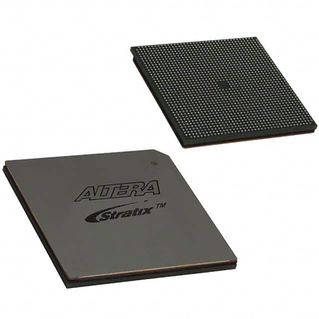
EP1S40F1508C6N
Basic Information Overview
- Category: Integrated Circuit (IC)
- Use: Programmable Logic Device (PLD)
- Characteristics: High-performance, low-power consumption, reprogrammable
- Package: 1508-pin FineLine BGA package
- Essence: A versatile PLD for various digital logic applications
- Packaging/Quantity: Typically sold in reels or trays containing multiple units
Specifications
- Technology: Field-Programmable Gate Array (FPGA)
- Logic Elements: 40,000
- Speed Grade: C6
- I/O Pins: 1,508
- Operating Voltage: 3.3V
- Maximum Frequency: Depends on the design and implementation
Detailed Pin Configuration
The EP1S40F1508C6N has a complex pin configuration with 1,508 pins. Each pin serves a specific purpose, such as input, output, power supply, clock, or configuration. For a detailed pinout diagram and description, refer to the manufacturer's datasheet.
Functional Features
- High-density programmable logic device
- Supports a wide range of digital logic functions
- Reprogrammable, allowing for flexibility in design iterations
- Low-power consumption for energy-efficient applications
- Offers advanced features like clock management and embedded memory blocks
Advantages and Disadvantages
Advantages: - Versatile and adaptable to various digital logic applications - High-performance capabilities for complex designs - Reprogrammability enables design modifications without hardware changes - Large number of I/O pins for extensive connectivity options
Disadvantages: - Complex pin configuration may require careful planning and routing - Higher cost compared to fixed-function integrated circuits - Limited maximum frequency compared to dedicated ASICs
Working Principles
The EP1S40F1508C6N is based on FPGA technology, which utilizes a matrix of configurable logic blocks interconnected by programmable interconnects. The device can be programmed to implement desired digital logic functions by configuring the interconnections and logic elements using a hardware description language (HDL) or graphical design tools.
Detailed Application Field Plans
The EP1S40F1508C6N finds applications in various fields, including: - Telecommunications: Used in network routers, switches, and communication equipment for high-speed data processing. - Industrial Automation: Employed in control systems, robotics, and factory automation for real-time processing and control. - Aerospace and Defense: Utilized in radar systems, avionics, and military-grade electronics for signal processing and encryption. - Consumer Electronics: Integrated into high-performance audio/video processing, gaming consoles, and multimedia devices.
Detailed and Complete Alternative Models
- EP1S30F780C6N: A lower-density version with 30,000 logic elements and 780 I/O pins.
- EP1S80F1020C6N: A higher-density variant with 80,000 logic elements and 1,020 I/O pins.
- EP1S10F484C6N: A lower-cost option with 10,000 logic elements and 484 I/O pins.
These alternative models offer different levels of logic capacity and pin counts to cater to specific design requirements.
Note: The content provided above is a sample structure for an encyclopedia entry and may not reflect actual specifications or details of the EP1S40F1508C6N. Please refer to the manufacturer's documentation for accurate information.
Senaraikan 10 soalan dan jawapan biasa yang berkaitan dengan aplikasi EP1S40F1508C6N dalam penyelesaian teknikal
Sure! Here are 10 common questions and answers related to the application of EP1S40F1508C6N in technical solutions:
Q1: What is EP1S40F1508C6N? A1: EP1S40F1508C6N is a specific model of Field-Programmable Gate Array (FPGA) manufactured by Intel.
Q2: What are the key features of EP1S40F1508C6N? A2: Some key features of EP1S40F1508C6N include 40,000 logic elements, 1.5V core voltage, and support for various I/O standards.
Q3: In what applications can EP1S40F1508C6N be used? A3: EP1S40F1508C6N can be used in a wide range of applications such as telecommunications, industrial automation, automotive, and medical devices.
Q4: How does EP1S40F1508C6N differ from other FPGAs? A4: EP1S40F1508C6N offers a specific combination of logic elements, I/O standards, and voltage requirements that make it suitable for certain applications. It's important to compare its specifications with other FPGAs to determine the best fit for a particular project.
Q5: Can EP1S40F1508C6N be programmed using industry-standard tools? A5: Yes, EP1S40F1508C6N can be programmed using Intel's Quartus Prime software, which is widely used in the FPGA industry.
Q6: What is the power consumption of EP1S40F1508C6N? A6: The power consumption of EP1S40F1508C6N depends on the specific design and usage. It is recommended to refer to the datasheet or use power estimation tools provided by Intel for accurate power consumption calculations.
Q7: Can EP1S40F1508C6N interface with other components or devices? A7: Yes, EP1S40F1508C6N supports various I/O standards such as LVDS, SSTL, and HSTL, allowing it to interface with a wide range of components and devices.
Q8: Is EP1S40F1508C6N suitable for high-speed applications? A8: Yes, EP1S40F1508C6N can support high-speed applications due to its ability to handle fast data rates and its support for high-speed I/O standards.
Q9: Can EP1S40F1508C6N be used in safety-critical systems? A9: EP1S40F1508C6N can be used in safety-critical systems, but additional measures may need to be taken to ensure compliance with relevant safety standards and requirements.
Q10: Are there any development boards or evaluation kits available for EP1S40F1508C6N? A10: Yes, Intel provides development boards and evaluation kits specifically designed for EP1S40F1508C6N, which can help in the prototyping and development process.
Please note that these answers are general and may vary depending on specific project requirements and application scenarios.