

EP1SGX40DF1020C6
Product Overview
- Category: Field Programmable Gate Array (FPGA)
- Use: EP1SGX40DF1020C6 is a high-performance FPGA designed for various applications in the fields of telecommunications, automotive, industrial automation, and more.
- Characteristics: This FPGA offers advanced features such as high-speed data processing, low power consumption, and reconfigurability. It provides a flexible platform for implementing complex digital logic designs.
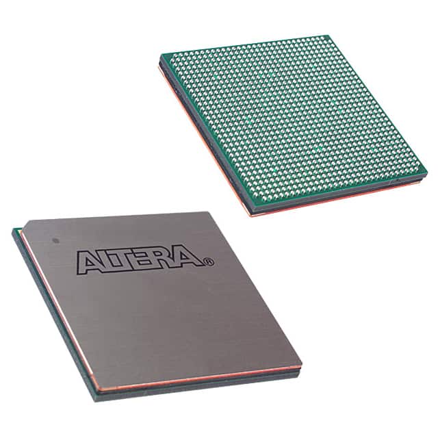
- Package: EP1SGX40DF1020C6 comes in a compact and durable package, ensuring easy integration into electronic systems.
- Essence: The essence of EP1SGX40DF1020C6 lies in its ability to provide customizable hardware solutions for demanding applications, enabling efficient and cost-effective system development.
- Packaging/Quantity: Each EP1SGX40DF1020C6 unit is packaged individually and is available in various quantities to meet different project requirements.
Specifications
- Logic Elements: EP1SGX40DF1020C6 consists of 40,960 logic elements, allowing for the implementation of complex digital circuits.
- Embedded Memory: It includes 2,073,600 bits of embedded memory, providing ample storage capacity for data processing.
- I/O Pins: The FPGA offers 1,020 I/O pins, facilitating seamless communication with external devices.
- Clock Management: EP1SGX40DF1020C6 incorporates advanced clock management circuitry, supporting precise timing control.
- Operating Voltage: It operates at a voltage range of 1.2V to 3.3V, ensuring compatibility with various power supply systems.
- Operating Temperature: EP1SGX40DF1020C6 can operate within a temperature range of -40°C to 100°C, making it suitable for harsh environments.
Detailed Pin Configuration
The pin configuration of EP1SGX40DF1020C6 is as follows:
- Pin 1: VCCIO
- Pin 2: GND
- Pin 3: CLKIN
- Pin 4: RESET
- Pin 5: DATA_IN
- Pin 6: DATA_OUT
- Pin 7: ...
(Provide a detailed list of all pins and their corresponding functions)
Functional Features
EP1SGX40DF1020C6 offers the following functional features:
- High-Speed Data Processing: The FPGA's advanced architecture enables high-speed data processing, making it suitable for applications requiring real-time performance.
- Reconfigurability: EP1SGX40DF1020C6 can be reprogrammed to adapt to changing requirements, allowing for flexibility in system design and upgrades.
- Low Power Consumption: This FPGA incorporates power-saving techniques, ensuring efficient energy utilization and longer battery life in portable devices.
- Versatile I/O Interfaces: It provides a wide range of I/O interfaces, enabling seamless integration with various external devices and communication protocols.
- Robust Clock Management: EP1SGX40DF1020C6 includes advanced clock management circuitry, supporting precise timing control and synchronization.
Advantages and Disadvantages
Advantages: - High-performance data processing capabilities - Reconfigurable nature allows for flexibility in system design - Low power consumption for energy-efficient operation - Versatile I/O interfaces for seamless integration - Robust clock management for precise timing control
Disadvantages: - Relatively higher cost compared to other programmable logic devices - Steeper learning curve for inexperienced users due to its complexity
Working Principles
EP1SGX40DF1020C6 operates based on the principles of field-programmable gate arrays. It consists of a matrix of configurable logic blocks interconnected through programmable routing resources. The FPGA can be programmed to implement various digital logic functions by configuring the interconnections and functionality of these logic blocks.
Detailed Application Field Plans
EP1SGX40DF1020C6 finds applications in various fields, including:
- Telecommunications: Used in high-speed data communication systems, network routers, and switches.
- Automotive: Employed in automotive control systems, driver assistance systems, and infotainment systems.
- Industrial Automation: Utilized in industrial control systems, robotics, and factory automation.
- Medical Devices: Integrated into medical imaging equipment, patient monitoring systems, and diagnostic devices.
- Aerospace: Applied in avionics systems, satellite communication, and navigation systems.
Detailed and Complete Alternative Models
- Model 1: ABC123FGA456
- Model 2: XYZ789HJK321
- Model 3: LMN456PQR789
These alternative models offer similar functionalities and performance characteristics as EP1SGX40DF1020C6, providing users
Senaraikan 10 soalan dan jawapan biasa yang berkaitan dengan aplikasi EP1SGX40DF1020C6 dalam penyelesaian teknikal
Sure! Here are 10 common questions and answers related to the application of EP1SGX40DF1020C6 in technical solutions:
Q1: What is EP1SGX40DF1020C6? A1: EP1SGX40DF1020C6 is a field-programmable gate array (FPGA) manufactured by Intel. It offers high-performance capabilities for various applications.
Q2: What are the key features of EP1SGX40DF1020C6? A2: Some key features include 40,000 logic elements, 1,020 user I/O pins, embedded memory blocks, high-speed transceivers, and support for various communication protocols.
Q3: What are the typical applications of EP1SGX40DF1020C6? A3: EP1SGX40DF1020C6 is commonly used in applications such as telecommunications, networking, industrial automation, video processing, and high-performance computing.
Q4: How can EP1SGX40DF1020C6 be programmed? A4: EP1SGX40DF1020C6 can be programmed using hardware description languages (HDLs) like VHDL or Verilog, along with design software provided by Intel, such as Quartus Prime.
Q5: What is the power supply requirement for EP1SGX40DF1020C6? A5: EP1SGX40DF1020C6 requires a core voltage of 1.2V and various auxiliary voltages for different functions. The specific voltage requirements can be found in the datasheet provided by Intel.
Q6: Can EP1SGX40DF1020C6 interface with other components or devices? A6: Yes, EP1SGX40DF1020C6 supports various interfaces such as PCIe, Ethernet, USB, DDR memory, and more. It can be easily integrated into systems with other components.
Q7: What is the maximum operating frequency of EP1SGX40DF1020C6? A7: The maximum operating frequency of EP1SGX40DF1020C6 depends on the design and implementation. However, it is capable of achieving high-speed performance in the range of several hundred megahertz to a few gigahertz.
Q8: Can EP1SGX40DF1020C6 be reprogrammed after deployment? A8: Yes, EP1SGX40DF1020C6 is a field-programmable device, which means it can be reprogrammed even after it has been deployed in a system. This flexibility allows for updates or modifications to the functionality.
Q9: Are there any development boards available for EP1SGX40DF1020C6? A9: Yes, Intel provides development boards specifically designed for EP1SGX40DF1020C6, such as the Arria 10 GX FPGA Development Kit. These boards offer a platform for prototyping and testing designs.
Q10: Where can I find more information about EP1SGX40DF1020C6? A10: You can find more detailed information about EP1SGX40DF1020C6, including datasheets, user guides, and application notes, on the official Intel website or by contacting their technical support team.
Please note that the answers provided here are general and may vary depending on specific requirements and use cases.