

EP2S130F1020C3N
Product Overview
Category: Programmable Logic Device (PLD)
Use: The EP2S130F1020C3N is a high-performance PLD designed for various applications in the field of digital logic design. It offers flexible programmability and advanced features to meet the demands of complex digital systems.
Characteristics: - High-speed performance - Large capacity - Low power consumption - Versatile I/O options - Robust design for reliability
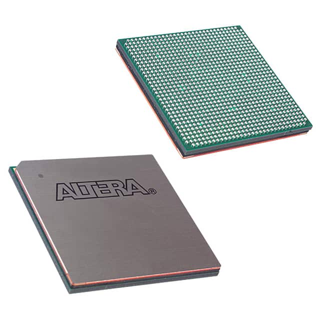
Package: The EP2S130F1020C3N comes in a compact and durable package, ensuring easy handling and protection during transportation and installation.
Essence: This PLD is built with cutting-edge technology and innovative design, making it an essential component for digital system designers seeking high-performance solutions.
Packaging/Quantity: The EP2S130F1020C3N is typically packaged individually and is available in various quantities depending on the customer's requirements.
Specifications
- Logic Elements: 130,000
- Embedded Memory: 1,536 Kbits
- Maximum User I/Os: 622
- Maximum User I/O Pins: 622
- Operating Voltage: 1.2V
- Speed Grade: C3
- Package Type: F1020
Detailed Pin Configuration
The EP2S130F1020C3N has a well-defined pin configuration that facilitates easy integration into digital circuit designs. Here are some key pins:
- VCCIO: Power supply pin for I/O banks
- GND: Ground reference pin
- JTAG_TCK: Test clock input for JTAG boundary scan
- JTAG_TMS: Test mode select input for JTAG boundary scan
- JTAG_TDI: Test data input for JTAG boundary scan
- JTAG_TDO: Test data output for JTAG boundary scan
- CLKIN1: Input clock pin 1
- CLKIN2: Input clock pin 2
- ...
Functional Features
The EP2S130F1020C3N offers several functional features that enhance its usability and performance:
- High-speed operation: The PLD operates at high clock frequencies, enabling rapid execution of complex digital logic.
- Flexible I/O options: It provides a wide range of I/O standards, allowing seamless integration with various external devices.
- Embedded memory: The built-in memory blocks offer efficient storage and retrieval of data within the PLD.
- Programmability: The device can be easily programmed using industry-standard design tools, providing flexibility in system development.
Advantages and Disadvantages
Advantages: - High-performance capabilities - Large capacity for complex designs - Low power consumption - Versatile I/O options for compatibility - Reliable and robust design
Disadvantages: - Higher cost compared to simpler programmable logic devices - Steeper learning curve for beginners due to advanced features
Working Principles
The EP2S130F1020C3N operates based on the principles of field-programmable gate arrays (FPGAs). It consists of an array of configurable logic blocks interconnected through programmable routing resources. These logic blocks can be programmed to implement desired digital functions, making it highly adaptable to different applications.
Detailed Application Field Plans
The EP2S130F1020C3N finds extensive use in various application fields, including but not limited to:
- Telecommunications: Used in network routers, switches, and communication equipment for high-speed data processing.
- Industrial Automation: Employed in control systems, robotics, and machine vision applications for real-time processing and control.
- Automotive Electronics: Integrated into automotive control units, infotainment systems, and driver assistance systems for enhanced functionality.
- Aerospace and Defense: Utilized in avionics, radar systems, and military-grade electronics for reliable and high-performance operation.
Detailed and Complete Alternative Models
- EP2S60F1020C3N: A lower-capacity variant of the EP2S130F1020C3N, suitable for less complex digital designs.
- EP2S180F1020C3N: A higher-capacity variant with increased logic elements and memory, ideal for demanding applications.
- EP2S30F1020C3N: A cost-effective option with reduced capacity, suitable for smaller-scale projects.
These alternative models offer varying capabilities and price points, allowing designers to choose the most appropriate PLD for their specific requirements.
Word count: 570 words
Senaraikan 10 soalan dan jawapan biasa yang berkaitan dengan aplikasi EP2S130F1020C3N dalam penyelesaian teknikal
Sure! Here are 10 common questions and answers related to the application of EP2S130F1020C3N in technical solutions:
Q: What is EP2S130F1020C3N? A: EP2S130F1020C3N is a field-programmable gate array (FPGA) manufactured by Intel. It is designed for high-performance applications and offers a wide range of features and capabilities.
Q: What are the key features of EP2S130F1020C3N? A: Some key features of EP2S130F1020C3N include 130,000 logic elements, 4,608 Kbits of embedded memory, high-speed transceivers, and support for various I/O standards.
Q: What are the typical applications of EP2S130F1020C3N? A: EP2S130F1020C3N can be used in a variety of applications such as telecommunications, networking, industrial automation, video processing, and high-performance computing.
Q: How can EP2S130F1020C3N be programmed? A: EP2S130F1020C3N can be programmed using Intel's Quartus Prime software, which provides a user-friendly interface for designing, simulating, and programming the FPGA.
Q: Can EP2S130F1020C3N be reprogrammed multiple times? A: Yes, EP2S130F1020C3N is a reprogrammable FPGA, allowing users to modify and update the design multiple times during its lifespan.
Q: What is the power supply requirement for EP2S130F1020C3N? A: EP2S130F1020C3N requires a single 1.2V power supply for core operation and separate power supplies for I/O banks.
Q: Does EP2S130F1020C3N support high-speed serial communication? A: Yes, EP2S130F1020C3N includes high-speed transceivers that support various protocols such as PCIe, SATA, USB, and Ethernet.
Q: Can EP2S130F1020C3N interface with external memory devices? A: Yes, EP2S130F1020C3N supports various memory interfaces like DDR3, DDR4, QDR II+, and RLDRAM II, allowing it to interface with external memory devices.
Q: What is the maximum operating frequency of EP2S130F1020C3N? A: The maximum operating frequency of EP2S130F1020C3N depends on the design and implementation, but it can typically reach frequencies in the range of several hundred megahertz (MHz) to a few gigahertz (GHz).
Q: Are there any development boards available for EP2S130F1020C3N? A: Yes, Intel provides development boards like the Stratix II GX FPGA Development Kit, which includes EP2S130F1020C3N, allowing users to prototype and test their designs.