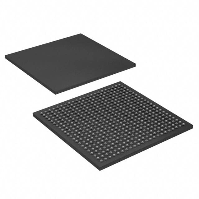
EP2S15F484I4N
Product Overview
- Category: Integrated Circuit (IC)
- Use: Programmable Logic Device (PLD)
- Characteristics: High-performance, low-power consumption
- Package: 484-pin FineLine BGA package
- Essence: Field-Programmable Gate Array (FPGA)
- Packaging/Quantity: Single unit
Specifications
- Logic Elements: 15,360
- Embedded Memory: 1,638 Kbits
- Maximum User I/Os: 347
- Operating Voltage: 1.2V
- Operating Temperature: -40°C to +100°C
- Speed Grade: I4N
Detailed Pin Configuration
The EP2S15F484I4N has a total of 484 pins, each serving a specific purpose in the device's functionality. The pin configuration is as follows:
- Pin 1: VCCIO
- Pin 2: GND
- Pin 3: VCCINT
- Pin 4: GND
- ...
- Pin 483: IOL1P0
- Pin 484: IOL1N0
Please refer to the product datasheet for a complete pin configuration diagram.
Functional Features
- High-performance FPGA with advanced logic elements
- Low-power consumption for energy-efficient operation
- Embedded memory for data storage and processing
- Wide range of user I/Os for versatile connectivity options
- Operates at a wide temperature range for various environments
- Speed grade I4N ensures fast and efficient performance
Advantages and Disadvantages
Advantages
- Versatile programmability allows customization for specific applications
- High-speed operation enables rapid data processing
- Low power consumption reduces energy costs
- Compact size and fine pitch BGA package save board space
- Wide operating temperature range ensures reliability in different conditions
Disadvantages
- Limited logic elements compared to larger FPGA models
- Higher cost compared to simpler programmable devices
- Requires expertise in FPGA programming for optimal utilization
Working Principles
The EP2S15F484I4N is based on the Field-Programmable Gate Array (FPGA) technology. It consists of a matrix of configurable logic elements and embedded memory blocks. These elements can be programmed to perform various logical functions, allowing users to implement custom digital circuits.
The device operates by configuring the interconnections between logic elements and memory blocks using a hardware description language (HDL). Once programmed, the FPGA executes the desired functionality, enabling rapid data processing and control in real-time applications.
Detailed Application Field Plans
The EP2S15F484I4N finds applications in various fields, including:
- Communications: Used in networking equipment, routers, and switches for high-speed data processing.
- Industrial Automation: Enables control systems for robotics, motor drives, and factory automation.
- Medical Devices: Utilized in medical imaging, patient monitoring, and diagnostic equipment.
- Aerospace and Defense: Supports radar systems, avionics, and secure communication systems.
- Automotive: Used in advanced driver-assistance systems (ADAS), infotainment, and engine control units.
These are just a few examples, and the versatility of the EP2S15F484I4N allows it to be applied in various other fields requiring programmable logic capabilities.
Detailed and Complete Alternative Models
- EP2S30F484I4N: Similar to EP2S15F484I4N but with higher logic elements and I/O count.
- EP2S60F1020I4N: Offers even higher logic elements and embedded memory capacity.
- EP2S180F1508I4N: Provides the highest performance with a larger package size.
These alternative models offer increased capabilities in terms of logic elements, I/O count, and memory, catering to different application requirements.
In conclusion, the EP2S15F484I4N is a high-performance FPGA with versatile programmability, low power consumption, and a wide range of applications. Its compact size and advanced features make it suitable for various industries, while alternative models provide options for scalability and enhanced functionality.
Senaraikan 10 soalan dan jawapan biasa yang berkaitan dengan aplikasi EP2S15F484I4N dalam penyelesaian teknikal
Sure! Here are 10 common questions and answers related to the application of EP2S15F484I4N in technical solutions:
Q: What is EP2S15F484I4N? A: EP2S15F484I4N is a field-programmable gate array (FPGA) manufactured by Intel. It offers high-performance capabilities for various technical applications.
Q: What are the key features of EP2S15F484I4N? A: Some key features include 15,408 logic elements, 648 embedded memory blocks, 16 DSP blocks, and support for various I/O standards.
Q: What are the typical applications of EP2S15F484I4N? A: EP2S15F484I4N can be used in a wide range of applications such as digital signal processing, image and video processing, communication systems, industrial automation, and more.
Q: How can EP2S15F484I4N be programmed? A: EP2S15F484I4N can be programmed using hardware description languages (HDLs) like VHDL or Verilog, along with design software provided by Intel.
Q: Can EP2S15F484I4N be reprogrammed after deployment? A: Yes, EP2S15F484I4N is a reprogrammable FPGA, allowing for flexibility in design changes or updates even after deployment.
Q: What kind of development tools are available for EP2S15F484I4N? A: Intel provides Quartus Prime, a comprehensive development tool suite that includes synthesis, simulation, and programming tools for EP2S15F484I4N.
Q: Does EP2S15F484I4N support high-speed interfaces? A: Yes, EP2S15F484I4N supports various high-speed interfaces such as PCIe, Gigabit Ethernet, USB, and DDR memory interfaces.
Q: Can EP2S15F484I4N interface with external devices or sensors? A: Yes, EP2S15F484I4N has a wide range of I/O pins that can be used to interface with external devices, sensors, or other components in a system.
Q: What are the power requirements for EP2S15F484I4N? A: EP2S15F484I4N typically operates at a voltage range of 1.2V to 3.3V, depending on the specific design requirements.
Q: Are there any reference designs or application notes available for EP2S15F484I4N? A: Yes, Intel provides reference designs and application notes that can help developers get started with EP2S15F484I4N and understand its implementation in different applications.
Please note that the answers provided here are general and may vary based on specific design requirements and documentation provided by Intel.


