

EP2S15F672C5
Product Overview
- Category: Integrated Circuit (IC)
- Use: Programmable Logic Device (PLD)
- Characteristics: High-performance, low-power consumption
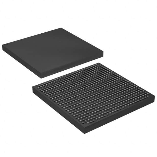
- Package: 672-ball FineLine BGA package
- Essence: Versatile programmable logic solution
- Packaging/Quantity: Single unit per package
Specifications
- Manufacturer: Intel Corporation
- Family: Stratix II
- Device Type: Field Programmable Gate Array (FPGA)
- Logic Elements: 15,360
- Embedded Memory: 1,008 Kbits
- Maximum User I/Os: 622
- Operating Voltage: 1.2V
- Operating Temperature: -40°C to +100°C
- Speed Grade: C5
Detailed Pin Configuration
The EP2S15F672C5 has a total of 672 pins arranged in a specific configuration. The pinout diagram and detailed pin descriptions can be found in the manufacturer's datasheet.
Functional Features
- High-performance FPGA with advanced architecture
- Flexible and reprogrammable logic elements
- Extensive embedded memory for data storage
- Support for various communication protocols
- Built-in high-speed transceivers for fast data transfer
- On-chip PLLs for clock management
- Dedicated DSP blocks for signal processing
- Comprehensive I/O capabilities for interfacing with external devices
Advantages and Disadvantages
Advantages: - Versatile and customizable logic solution - High-performance and low-power consumption - Large embedded memory capacity - Support for various communication protocols - Suitable for a wide range of applications
Disadvantages: - Relatively high cost compared to other programmable logic devices - Complex programming and design flow - Limited availability of alternative models
Working Principles
The EP2S15F672C5 is based on the field-programmable gate array (FPGA) technology. It consists of a large number of configurable logic blocks interconnected through programmable routing resources. The device can be programmed to implement various digital circuits and functions by configuring the interconnections and functionality of its logic elements.
Detailed Application Field Plans
The EP2S15F672C5 is widely used in applications that require high-performance and flexible digital logic solutions. Some common application fields include:
- Telecommunications: Used in network routers, switches, and communication equipment for data processing and protocol handling.
- Industrial Automation: Employed in control systems, robotics, and factory automation for real-time data processing and control.
- Aerospace and Defense: Utilized in radar systems, avionics, and military-grade equipment for signal processing and communication.
- Medical Devices: Integrated into medical imaging systems, patient monitoring devices, and diagnostic equipment for data processing and analysis.
- Automotive Electronics: Incorporated in advanced driver assistance systems (ADAS), infotainment systems, and engine control units (ECUs) for various functionalities.
Detailed and Complete Alternative Models
While the EP2S15F672C5 is a highly capable FPGA, there are alternative models available from other manufacturers that offer similar features and performance. Some notable alternatives include:
- Xilinx Virtex-7 XC7VX690T: A high-end FPGA with 690K logic cells and extensive I/O capabilities.
- Lattice Semiconductor ECP5-85: A low-power FPGA with 84K look-up tables (LUTs) and built-in SERDES channels.
- Microsemi SmartFusion2 M2S150: A mixed-signal FPGA with integrated ARM Cortex-M3 processor and security features.
These alternative models provide options for designers based on specific requirements and preferences.
Word count: 410 words
Senaraikan 10 soalan dan jawapan biasa yang berkaitan dengan aplikasi EP2S15F672C5 dalam penyelesaian teknikal
Sure! Here are 10 common questions and answers related to the application of EP2S15F672C5 in technical solutions:
Q: What is EP2S15F672C5? A: EP2S15F672C5 is a field-programmable gate array (FPGA) manufactured by Intel (formerly Altera). It is part of the Stratix II family of FPGAs.
Q: What are the key features of EP2S15F672C5? A: EP2S15F672C5 offers 15,360 logic elements, 672 embedded memory blocks, 672 DSP blocks, and various I/O options. It also supports high-speed serial transceivers and has built-in configuration capabilities.
Q: What applications can EP2S15F672C5 be used for? A: EP2S15F672C5 can be used in a wide range of applications, including telecommunications, networking, industrial automation, video processing, and high-performance computing.
Q: How do I program EP2S15F672C5? A: EP2S15F672C5 can be programmed using the Quartus Prime software provided by Intel. The programming file generated by Quartus Prime can be loaded onto the FPGA using a programming device or through JTAG interface.
Q: Can EP2S15F672C5 be reprogrammed multiple times? A: Yes, EP2S15F672C5 is a reprogrammable FPGA. You can modify and reprogram it as many times as needed during the development and testing phases.
Q: What voltage levels does EP2S15F672C5 support? A: EP2S15F672C5 supports both 3.3V and 2.5V voltage levels for its I/O pins, allowing compatibility with a wide range of external devices.
Q: Does EP2S15F672C5 have any built-in security features? A: Yes, EP2S15F672C5 provides various security features like bitstream encryption, design separation, and configuration protection to safeguard the intellectual property (IP) implemented on the FPGA.
Q: Can EP2S15F672C5 interface with other components or devices? A: Yes, EP2S15F672C5 supports various communication protocols such as PCIe, Ethernet, USB, SPI, I2C, and UART, enabling seamless integration with other components or devices in a system.
Q: What kind of performance can be expected from EP2S15F672C5? A: EP2S15F672C5 offers high-performance capabilities with fast logic processing, efficient memory utilization, and dedicated DSP blocks for signal processing tasks.
Q: Are there any development boards available for EP2S15F672C5? A: Yes, Intel provides development kits like the Stratix II GX FPGA Development Kit that includes EP2S15F672C5, allowing developers to quickly prototype and evaluate their designs.
Please note that the specific details and answers may vary depending on the context and requirements of your technical solution.