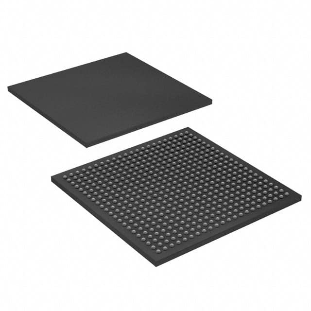
EP2S30F484I4N
Product Overview
Category
EP2S30F484I4N belongs to the category of Field Programmable Gate Arrays (FPGAs).
Use
This FPGA is commonly used in various electronic applications that require high-performance digital logic circuits.
Characteristics
- High-speed and flexible programmability
- Large number of configurable logic blocks
- Integrated memory blocks for data storage
- Support for complex digital signal processing algorithms
- Low power consumption
- High reliability and durability
Package
EP2S30F484I4N is available in a compact and durable package, designed to withstand harsh environmental conditions.
Essence
The essence of EP2S30F484I4N lies in its ability to provide a versatile platform for implementing custom digital logic designs.
Packaging/Quantity
This FPGA is typically sold individually or in small quantities, depending on the requirements of the user.
Specifications
- Device Type: Field Programmable Gate Array (FPGA)
- Model Number: EP2S30F484I4N
- Logic Elements: 30,000
- Embedded Memory: 1,500 Kbits
- Maximum Operating Frequency: 400 MHz
- I/O Pins: 484
- Power Supply Voltage: 1.2V
- Package Type: BGA (Ball Grid Array)
Detailed Pin Configuration
The EP2S30F484I4N FPGA has a total of 484 pins, which are divided into different categories based on their functionality. The pin configuration includes:
- Input/Output (I/O) pins: These pins are used for communication with external devices and can be configured as either input or output.
- Clock pins: These pins provide the necessary clock signals for synchronous operation.
- Power supply pins: These pins are used to provide the required voltage levels for proper functioning of the FPGA.
- Configuration pins: These pins are used for programming and configuring the FPGA.
Functional Features
- High-speed data processing capabilities
- Support for various communication protocols
- On-chip memory blocks for efficient data storage
- Flexible I/O configurations
- Built-in digital signal processing (DSP) blocks for complex algorithms
- Configurable clock management resources
- Support for partial reconfiguration
Advantages and Disadvantages
Advantages
- Versatile and flexible platform for implementing custom digital logic designs
- High-performance computing capabilities
- Low power consumption compared to traditional ASICs (Application-Specific Integrated Circuits)
- Shorter development time due to programmability
- Cost-effective solution for prototyping and low-volume production
Disadvantages
- Limited scalability compared to ASICs for high-volume production
- Higher cost per unit compared to mass-produced integrated circuits
- Requires specialized knowledge and expertise for design and programming
Working Principles
EP2S30F484I4N operates based on the principles of reconfigurable computing. It consists of a large number of configurable logic blocks interconnected through programmable routing resources. The user can program these logic blocks to implement desired digital logic functions. The configuration data is stored in on-chip memory or loaded from external sources during startup.
The FPGA can be reprogrammed multiple times, allowing for flexibility in design modifications and updates without the need for hardware changes.
Detailed Application Field Plans
EP2S30F484I4N finds applications in various fields, including:
- Telecommunications: Used in base stations, network routers, and switches for high-speed data processing and protocol handling.
- Industrial Automation: Employed in control systems, motor drives, and robotics for real-time control and signal processing.
- Aerospace and Defense: Utilized in radar systems, avionics, and satellite communication for high-performance signal processing and data handling.
- Medical Electronics: Applied in medical imaging, patient monitoring, and diagnostic equipment for high-speed data processing and image analysis.
- Automotive: Used in advanced driver assistance systems (ADAS), infotainment systems, and engine control units for real-time processing and control.
Detailed and Complete Alternative Models
- EP2S60F484I4N: Similar to EP2S30F484I4N but with higher logic capacity and more I/O pins.
- EP2S15F484I4N: A lower-cost alternative with reduced logic capacity and fewer I/O pins.
- EP2S90F484I4N: A higher-performance option with increased logic capacity and additional DSP blocks.
These alternative models provide varying levels of performance and functionality, allowing users to choose the most suitable FPGA for their specific requirements.
Word count: 660 words
Senaraikan 10 soalan dan jawapan biasa yang berkaitan dengan aplikasi EP2S30F484I4N dalam penyelesaian teknikal
Sure! Here are 10 common questions and answers related to the application of EP2S30F484I4N in technical solutions:
Q: What is EP2S30F484I4N? A: EP2S30F484I4N is a specific model of Field-Programmable Gate Array (FPGA) manufactured by Intel.
Q: What are the key features of EP2S30F484I4N? A: EP2S30F484I4N offers 30,000 logic elements, 1,080 Kbits of embedded memory, and various I/O interfaces for versatile applications.
Q: What are some typical applications of EP2S30F484I4N? A: EP2S30F484I4N is commonly used in digital signal processing, high-speed data acquisition, image and video processing, and communication systems.
Q: How can EP2S30F484I4N be programmed? A: EP2S30F484I4N can be programmed using Hardware Description Languages (HDLs) such as VHDL or Verilog, along with design software like Quartus Prime.
Q: Can EP2S30F484I4N be reprogrammed after initial programming? A: Yes, EP2S30F484I4N is a reprogrammable FPGA, allowing for updates and modifications to the design even after deployment.
Q: What are the power requirements for EP2S30F484I4N? A: EP2S30F484I4N typically operates at a voltage range of 1.2V to 3.3V, depending on the specific design requirements.
Q: Does EP2S30F484I4N support different communication protocols? A: Yes, EP2S30F484I4N supports various communication protocols such as UART, SPI, I2C, and Ethernet, making it suitable for interfacing with other devices.
Q: Can EP2S30F484I4N interface with external memory devices? A: Yes, EP2S30F484I4N has dedicated pins and interfaces to connect with external memory devices like DDR SDRAM or Flash memory.
Q: What development boards are available for EP2S30F484I4N? A: Intel provides development boards like the DE2 series that are compatible with EP2S30F484I4N, offering a platform for prototyping and testing.
Q: Are there any online resources or communities for EP2S30F484I4N users? A: Yes, Intel's website provides documentation, application notes, and forums where users can find support and interact with other FPGA enthusiasts.
Please note that the specific details and answers may vary depending on the context and requirements of the technical solution.


