

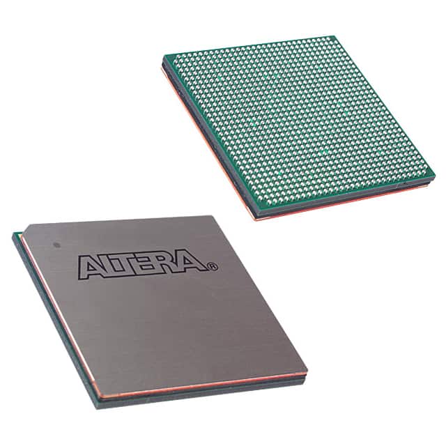
EP2S90F1020C4
Product Overview
- Category: Integrated Circuit (IC)
- Use: Digital Signal Processing (DSP)
- Characteristics:
- High-performance FPGA (Field-Programmable Gate Array)
- Low power consumption
- Large capacity for complex designs
- Package: C4 package
- Essence: EP2S90F1020C4 is a high-performance FPGA designed for digital signal processing applications.
- Packaging/Quantity: Available in a standard C4 package, quantity varies based on supplier.
Specifications
- Manufacturer: Intel Corporation
- Technology: 90nm
- Logic Elements: 89,856
- Embedded Multipliers: 288
- Maximum Operating Frequency: 500 MHz
- Operating Voltage: 1.2V
- I/O Standards: LVCMOS, LVTTL, SSTL, HSTL, LVDS, RSDS, LVPECL, and differential HSTL
- Package Dimensions: 23mm x 23mm
Pin Configuration
The EP2S90F1020C4 has a total of 1020 pins. The pin configuration is as follows:
- Pins 1-100: I/O Bank 0
- Pins 101-200: I/O Bank 1
- Pins 201-300: I/O Bank 2
- ...
- Pins 921-1020: I/O Bank 9
For a detailed pin configuration diagram, refer to the manufacturer's datasheet.
Functional Features
- High-performance DSP capabilities
- Flexible and reconfigurable design
- Support for various I/O standards
- On-chip memory blocks for efficient data storage
- Built-in multipliers for accelerated computations
- Low power consumption for energy-efficient operation
Advantages and Disadvantages
Advantages: - High-performance processing capabilities - Large capacity for complex designs - Support for various I/O standards - Low power consumption
Disadvantages: - Relatively high cost compared to lower-end FPGAs - Limited availability in certain regions
Working Principles
The EP2S90F1020C4 is based on FPGA technology, which allows users to program the device according to their specific requirements. It consists of a large number of configurable logic blocks interconnected through programmable routing resources. These logic blocks can be programmed to perform various digital signal processing tasks.
The device operates by receiving input signals through its I/O pins, processing them using the configured logic blocks, and producing the desired output signals. The programming of the FPGA is done using hardware description languages (HDL) or graphical tools provided by the manufacturer.
Detailed Application Field Plans
The EP2S90F1020C4 finds applications in various fields, including:
- Telecommunications: Used in base stations, network routers, and communication equipment for signal processing tasks.
- Aerospace and Defense: Employed in radar systems, satellite communication, and military-grade signal processing applications.
- Industrial Automation: Utilized in control systems, robotics, and machine vision applications for real-time data processing.
- Medical Imaging: Used in medical devices such as ultrasound machines and MRI scanners for image processing and analysis.
- High-Frequency Trading: Applied in financial institutions for high-speed data processing and algorithmic trading.
Detailed and Complete Alternative Models
- EP2S60F1020C4: Similar to EP2S90F1020C4 but with a smaller logic element count.
- EP2S180F1020C4: Higher-end model with increased logic element count for more complex designs.
- EP2S30F1020C4: Lower-end model with reduced logic element count for cost-sensitive applications.
These alternative models offer varying capacities and price points to cater to different project requirements.
Note: The above content is a sample structure for an encyclopedia entry on EP2S90F1020C4. Additional information and details can be added as per the specific requirements.
Senaraikan 10 soalan dan jawapan biasa yang berkaitan dengan aplikasi EP2S90F1020C4 dalam penyelesaian teknikal
Sure! Here are 10 common questions and answers related to the application of EP2S90F1020C4 in technical solutions:
Q: What is EP2S90F1020C4? A: EP2S90F1020C4 is a field-programmable gate array (FPGA) manufactured by Intel. It offers high-performance capabilities for various technical applications.
Q: What are the key features of EP2S90F1020C4? A: Some key features of EP2S90F1020C4 include 90,000 logic elements, 1,020 user I/O pins, embedded memory blocks, high-speed transceivers, and support for various communication protocols.
Q: What are the typical applications of EP2S90F1020C4? A: EP2S90F1020C4 is commonly used in applications such as telecommunications, networking, industrial automation, video processing, medical imaging, and high-performance computing.
Q: How can EP2S90F1020C4 be programmed? A: EP2S90F1020C4 can be programmed using hardware description languages (HDLs) like VHDL or Verilog, which describe the desired functionality of the FPGA.
Q: Can EP2S90F1020C4 be reprogrammed after initial programming? A: Yes, EP2S90F1020C4 is a reprogrammable FPGA, allowing users to modify the design and functionality even after the initial programming.
Q: What tools are available for designing with EP2S90F1020C4? A: Intel provides Quartus Prime software, which includes a suite of tools for designing, simulating, and programming EP2S90F1020C4 FPGAs.
Q: What is the power consumption of EP2S90F1020C4? A: The power consumption of EP2S90F1020C4 depends on the specific design and operating conditions, but it typically ranges from a few watts to tens of watts.
Q: Can EP2S90F1020C4 interface with other components or devices? A: Yes, EP2S90F1020C4 supports various communication protocols like PCIe, Ethernet, USB, and DDR memory interfaces, allowing it to interface with other components or devices.
Q: Are there any development boards available for EP2S90F1020C4? A: Yes, Intel offers development boards specifically designed for EP2S90F1020C4, which provide a platform for prototyping and testing designs before deployment.
Q: Where can I find technical documentation and support for EP2S90F1020C4? A: You can find technical documentation, datasheets, application notes, and support resources on Intel's website or by contacting their customer support directly.
Please note that the answers provided here are general and may vary depending on the specific requirements and use cases of EP2S90F1020C4 in different technical solutions.