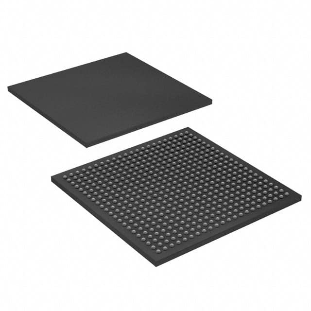
EP3C40U484C7N
Product Overview
- Category: Programmable Logic Device (PLD)
- Use: EP3C40U484C7N is a PLD used for digital logic design and implementation.
- Characteristics:
- High-performance device with low power consumption
- Offers high-speed data processing capabilities
- Provides flexibility in designing complex digital circuits
- Package: The EP3C40U484C7N comes in a 484-pin plastic quad flat pack (PQFP) package.
- Essence: EP3C40U484C7N is an essential component for building advanced digital systems.
- Packaging/Quantity: Typically sold in reels or trays, with each reel/tray containing a specific quantity of EP3C40U484C7N devices.
Specifications
- Logic Elements: The EP3C40U484C7N contains 40,000 logic elements.
- Memory: It has 1,152 Kbits of embedded memory.
- PLLs: The device features four phase-locked loops (PLLs).
- I/O Pins: EP3C40U484C7N offers 346 user I/O pins.
- Operating Voltage: It operates at a voltage range of 1.15V to 1.25V.
- Speed Grade: The speed grade of this PLD is -7, indicating a maximum operating frequency of 250 MHz.
Detailed Pin Configuration
The EP3C40U484C7N has a total of 484 pins, each serving a specific purpose in the device's functionality. A detailed pin configuration diagram can be found in the product datasheet.
Functional Features
- High-Speed Data Processing: EP3C40U484C7N enables rapid data processing due to its high-performance architecture.
- Flexibility: The device allows designers to implement complex digital circuits with ease, providing flexibility in system design.
- Low Power Consumption: EP3C40U484C7N is designed to minimize power consumption, making it suitable for energy-efficient applications.
Advantages and Disadvantages
Advantages: - High-performance capabilities - Flexibility in designing complex circuits - Low power consumption
Disadvantages: - Limited availability of alternative models - Higher cost compared to simpler logic devices
Working Principles
EP3C40U484C7N operates based on the principles of programmable logic. It consists of configurable logic blocks (CLBs), interconnect resources, embedded memory, and I/O elements. The device can be programmed using hardware description languages (HDLs) or schematic entry tools to define the desired digital circuit functionality.
Detailed Application Field Plans
EP3C40U484C7N finds application in various fields, including but not limited to: - Telecommunications - Industrial automation - Automotive electronics - Consumer electronics - Medical devices
In these fields, the PLD is used for tasks such as signal processing, control systems, data acquisition, and more.
Detailed and Complete Alternative Models
While EP3C40U484C7N is a popular choice for many applications, there are alternative models available from different manufacturers. Some notable alternatives include: - Xilinx XC3S400 - Altera Cyclone III EP3C25 - Lattice Semiconductor iCE40UP5K
These alternatives offer similar functionalities and can be considered depending on specific project requirements.
Word count: 315 words
Senaraikan 10 soalan dan jawapan biasa yang berkaitan dengan aplikasi EP3C40U484C7N dalam penyelesaian teknikal
Sure! Here are 10 common questions and answers related to the application of EP3C40U484C7N in technical solutions:
Q: What is EP3C40U484C7N? A: EP3C40U484C7N is a specific model of Field-Programmable Gate Array (FPGA) manufactured by Altera.
Q: What are the key features of EP3C40U484C7N? A: Some key features of EP3C40U484C7N include 40,000 logic elements, 484 user I/O pins, and support for various communication protocols.
Q: How can EP3C40U484C7N be used in technical solutions? A: EP3C40U484C7N can be used in a wide range of applications such as digital signal processing, embedded systems, and high-performance computing.
Q: What programming languages are supported by EP3C40U484C7N? A: EP3C40U484C7N can be programmed using Hardware Description Languages (HDLs) like VHDL or Verilog.
Q: Can EP3C40U484C7N be reprogrammed after deployment? A: Yes, EP3C40U484C7N is a reprogrammable FPGA, allowing for flexibility and updates to the design even after deployment.
Q: What tools are available for designing with EP3C40U484C7N? A: Altera provides Quartus Prime software, which includes tools for designing, simulating, and programming EP3C40U484C7N.
Q: Are there any development boards available for EP3C40U484C7N? A: Yes, Altera offers development boards like the DE0-Nano board that can be used for prototyping and testing with EP3C40U484C7N.
Q: Can EP3C40U484C7N interface with other components or devices? A: Yes, EP3C40U484C7N supports various communication protocols like UART, SPI, I2C, and Ethernet, allowing it to interface with other components or devices.
Q: What are some advantages of using EP3C40U484C7N in technical solutions? A: Some advantages include high performance, flexibility, low power consumption, and the ability to implement complex algorithms or functions.
Q: Are there any limitations or considerations when using EP3C40U484C7N? A: Some considerations include the need for expertise in FPGA design, potential resource limitations depending on the complexity of the design, and the cost compared to other solutions.
Please note that the specific questions and answers may vary based on the context and requirements of the technical solution.


