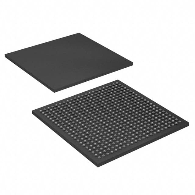
EP3SL50F484C2N
Product Overview
- Category: Programmable Logic Device (PLD)
- Use: EP3SL50F484C2N is a high-performance PLD designed for various applications in the field of digital logic design and implementation.
- Characteristics: The device offers advanced features such as high-speed performance, low power consumption, and flexible programmability.
- Package: EP3SL50F484C2N comes in a 484-pin FineLine BGA package.
- Essence: It serves as a versatile solution for implementing complex digital logic circuits with high speed and efficiency.
- Packaging/Quantity: The product is typically sold individually or in small quantities.
Specifications
- Logic Elements: EP3SL50F484C2N consists of 50,000 logic elements, providing ample resources for complex designs.
- Memory: It includes embedded memory blocks for storing data efficiently.
- I/O Pins: The device offers 484 I/O pins for interfacing with external components.
- Clocking: EP3SL50F484C2N supports multiple clocking options, allowing precise synchronization of operations.
- Power Consumption: The PLD is designed to operate at low power levels, ensuring energy efficiency.
Pin Configuration
The detailed pin configuration of EP3SL50F484C2N can be found in the manufacturer's datasheet. It provides a comprehensive overview of the pin assignments and their functions.
Functional Features
- High-Speed Performance: EP3SL50F484C2N operates at high clock frequencies, enabling rapid execution of complex logic operations.
- Flexibility: The device offers extensive programmability, allowing designers to implement custom logic functions tailored to specific requirements.
- Integration: EP3SL50F484C2N integrates various components such as logic elements, memory blocks, and I/O pins into a single device, simplifying system design.
- Reliability: The PLD is designed to provide reliable operation in demanding environments, ensuring consistent performance.
Advantages and Disadvantages
Advantages: - High-performance capabilities - Low power consumption - Flexible programmability - Integration of multiple components
Disadvantages: - Limited availability of alternative models - Steep learning curve for beginners
Working Principles
EP3SL50F484C2N operates based on the principles of programmable logic. It utilizes configurable logic elements and memory blocks to implement desired logic functions. The device can be programmed using hardware description languages or specialized software tools provided by the manufacturer.
Application Field Plans
EP3SL50F484C2N finds applications in various fields, including: - Telecommunications: Used in network infrastructure equipment for high-speed data processing. - Industrial Automation: Employed in control systems for efficient and flexible automation. - Aerospace: Utilized in avionics systems for reliable and high-performance digital signal processing. - Consumer Electronics: Integrated into multimedia devices for advanced functionality.
Alternative Models
While EP3SL50F484C2N is a highly capable PLD, there are alternative models available from other manufacturers that offer similar features. Some popular alternatives include: - Xilinx Virtex-7 series - Altera Cyclone V series - Lattice ECP5 series
These alternative models provide designers with options to choose the most suitable PLD based on their specific requirements.
Word count: 380 words
Senaraikan 10 soalan dan jawapan biasa yang berkaitan dengan aplikasi EP3SL50F484C2N dalam penyelesaian teknikal
Sure! Here are 10 common questions and answers related to the application of EP3SL50F484C2N in technical solutions:
Q: What is EP3SL50F484C2N? A: EP3SL50F484C2N is a specific model of FPGA (Field-Programmable Gate Array) manufactured by Intel.
Q: What are the key features of EP3SL50F484C2N? A: Some key features of EP3SL50F484C2N include 50,000 logic elements, 484-pin package, and support for various I/O standards.
Q: What are the typical applications of EP3SL50F484C2N? A: EP3SL50F484C2N can be used in a wide range of applications such as industrial automation, telecommunications, medical devices, and automotive systems.
Q: How can EP3SL50F484C2N be programmed? A: EP3SL50F484C2N can be programmed using hardware description languages (HDLs) like VHDL or Verilog, and then configured using programming tools provided by Intel.
Q: Can EP3SL50F484C2N be reprogrammed after initial configuration? A: Yes, EP3SL50F484C2N is a reprogrammable FPGA, allowing for multiple configurations during its lifetime.
Q: What kind of peripherals can be interfaced with EP3SL50F484C2N? A: EP3SL50F484C2N supports various communication interfaces such as UART, SPI, I2C, Ethernet, and USB, enabling integration with a wide range of peripherals.
Q: Does EP3SL50F484C2N have built-in memory? A: EP3SL50F484C2N does not have built-in memory, but it can be interfaced with external memory devices like DDR SDRAM or Flash memory.
Q: What is the power supply requirement for EP3SL50F484C2N? A: EP3SL50F484C2N typically operates at a voltage range of 1.2V to 3.3V, depending on the specific design requirements.
Q: Can EP3SL50F484C2N be used in safety-critical applications? A: Yes, EP3SL50F484C2N can be used in safety-critical applications, provided that proper design and verification processes are followed.
Q: Are there any development boards available for EP3SL50F484C2N? A: Yes, Intel provides development boards specifically designed for EP3SL50F484C2N, which include necessary interfaces and peripherals for prototyping and testing.
Please note that the answers provided here are general and may vary based on specific design requirements and application scenarios.


