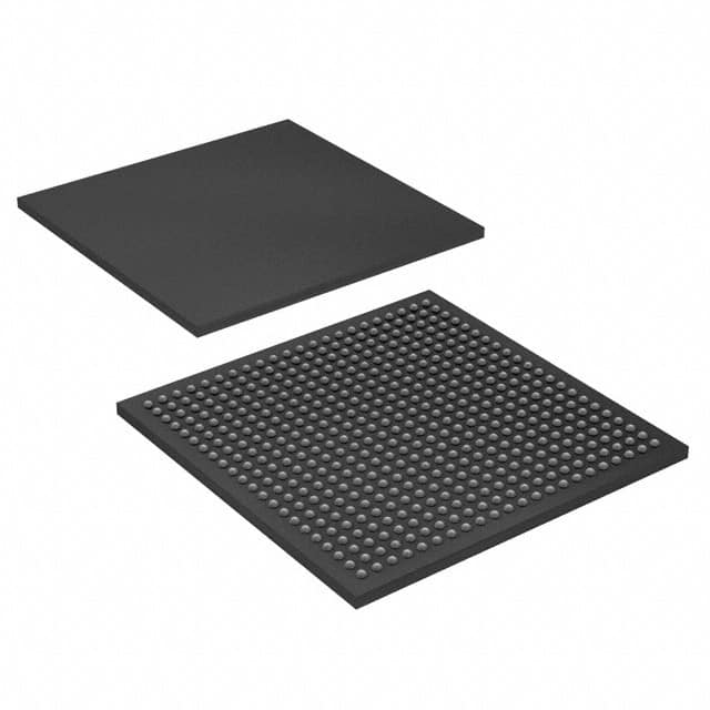
EP3SL50F484I3N
Product Overview
- Category: Programmable Logic Device (PLD)
- Use: EP3SL50F484I3N is a PLD used for digital logic design and implementation.
- Characteristics:
- High-performance device with low power consumption
- Offers high-speed data processing capabilities
- Provides flexibility in designing complex digital circuits
- Package: The EP3SL50F484I3N comes in a 484-pin FineLine BGA package.
- Essence: EP3SL50F484I3N is an advanced programmable logic device that enables the implementation of complex digital logic designs.
Specifications
- Logic Elements: 50,000
- Embedded Memory: 1,536 Kbits
- Maximum User I/Os: 346
- Clock Networks: 8
- PLLs: 4
- Maximum Operating Frequency: 400 MHz
- Supply Voltage: 1.2V
- Operating Temperature Range: -40°C to +100°C
Pin Configuration
The EP3SL50F484I3N has a detailed pin configuration as follows:

Functional Features
- High-speed data processing capabilities enable efficient execution of complex algorithms.
- Flexible I/O options allow easy integration with external devices.
- Advanced clock management features ensure precise timing control.
- On-chip memory resources provide storage for intermediate results and data buffering.
- Support for various communication protocols enhances connectivity options.
Advantages
- High-performance device suitable for demanding applications.
- Low power consumption helps reduce energy costs.
- Versatile and flexible design options enable customization for specific requirements.
- Extensive on-chip resources minimize the need for external components.
- Reliable operation over a wide temperature range ensures suitability for various environments.
Disadvantages
- Complex programming and design flow may require a steep learning curve for beginners.
- Limited availability of alternative models from other manufacturers.
- Higher cost compared to simpler programmable logic devices.
Working Principles
The EP3SL50F484I3N utilizes a combination of configurable logic blocks, embedded memory, and interconnect resources to implement digital logic designs. The device is programmed using hardware description languages (HDL) such as VHDL or Verilog. The programmed configuration is stored in non-volatile memory within the device and can be reprogrammed as needed.
During operation, the device executes the programmed logic by routing signals through the configurable logic blocks and interconnect resources. The embedded memory provides storage for intermediate results and data buffering. Clock management features ensure precise timing control, enabling synchronous operation of the circuit.
Application Field Plans
The EP3SL50F484I3N finds applications in various fields, including:
- Telecommunications: Used in base stations, network switches, and routers for high-speed data processing.
- Industrial Automation: Enables control and monitoring of complex manufacturing processes.
- Automotive: Utilized in advanced driver assistance systems (ADAS) and infotainment systems.
- Aerospace: Used in avionics systems for reliable and efficient data processing.
- Medical Devices: Enables the implementation of sophisticated medical imaging and diagnostic equipment.
Alternative Models
While the EP3SL50F484I3N is a highly capable PLD, there are alternative models available from other manufacturers that offer similar functionality. Some notable alternatives include:
- Xilinx Spartan-6 XC6SLX150T
- Altera Cyclone IV EP4CE115F29C7
- Lattice ECP5-85
- Microsemi SmartFusion2 M2S050T
These alternative models provide comparable performance and features, allowing designers to choose the most suitable option for their specific requirements.
In conclusion, the EP3SL50F484I3N is a high-performance programmable logic device with advanced features and flexibility. Its wide range of applications, combined with its reliable operation and extensive resources, make it a popular choice for digital logic design and implementation.
Senaraikan 10 soalan dan jawapan biasa yang berkaitan dengan aplikasi EP3SL50F484I3N dalam penyelesaian teknikal
Sure! Here are 10 common questions and answers related to the application of EP3SL50F484I3N in technical solutions:
Q: What is EP3SL50F484I3N? A: EP3SL50F484I3N is a specific model of Field-Programmable Gate Array (FPGA) manufactured by Intel.
Q: What are the key features of EP3SL50F484I3N? A: Some key features of EP3SL50F484I3N include 50,000 logic elements, 484-pin package, and support for various I/O standards.
Q: In what applications can EP3SL50F484I3N be used? A: EP3SL50F484I3N can be used in a wide range of applications such as industrial automation, telecommunications, automotive, and medical devices.
Q: How does EP3SL50F484I3N benefit technical solutions? A: EP3SL50F484I3N offers high-performance processing capabilities, flexibility, and reconfigurability, making it suitable for complex and evolving technical solutions.
Q: Can EP3SL50F484I3N be programmed using industry-standard design tools? A: Yes, EP3SL50F484I3N can be programmed using popular design tools like Quartus Prime, which provide a user-friendly interface for designing FPGA-based solutions.
Q: Does EP3SL50F484I3N support communication protocols? A: Yes, EP3SL50F484I3N supports various communication protocols such as UART, SPI, I2C, Ethernet, and PCIe, enabling seamless integration with other devices.
Q: Can EP3SL50F484I3N handle real-time processing requirements? A: Yes, EP3SL50F484I3N offers high-speed performance and low-latency capabilities, making it suitable for real-time processing applications.
Q: Is EP3SL50F484I3N power-efficient? A: Yes, EP3SL50F484I3N is designed to be power-efficient, allowing for optimized energy consumption in technical solutions.
Q: Can EP3SL50F484I3N be used in safety-critical applications? A: Yes, EP3SL50F484I3N supports various safety features like error correction codes (ECC) and built-in self-test (BIST), making it suitable for safety-critical applications.
Q: Are there any development resources available for EP3SL50F484I3N? A: Yes, Intel provides comprehensive documentation, reference designs, and support forums to assist developers in utilizing EP3SL50F484I3N effectively in their technical solutions.
Please note that the specific details and answers may vary depending on the context and requirements of each application.


