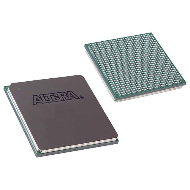
EP4CE40F29C9LN
Product Overview
- Category: Programmable Logic Device (PLD)
- Use: EP4CE40F29C9LN is a high-performance PLD that can be programmed to perform various logic functions.
- Characteristics:
- High-speed performance
- Low power consumption
- Large capacity
- Flexible and reprogrammable
- Package: The EP4CE40F29C9LN comes in a compact and durable package.
- Essence: EP4CE40F29C9LN is designed to provide efficient and customizable logic processing capabilities.
- Packaging/Quantity: The product is typically sold individually or in small quantities.
Specifications
- Logic Elements: 39,600
- Embedded Memory: 1,638 Kbits
- Maximum User I/O Pins: 202
- Operating Voltage: 1.2V
- Speed Grade: 9
- Package Type: FBGA
- Package Pins: 324
Detailed Pin Configuration
The EP4CE40F29C9LN has a total of 324 pins, which are used for various purposes such as input, output, power supply, and configuration. The detailed pin configuration can be found in the product datasheet.
Functional Features
- High-speed operation: The EP4CE40F29C9LN offers fast logic processing capabilities, making it suitable for applications that require real-time data processing.
- Low power consumption: The device is designed to minimize power consumption, making it energy-efficient and suitable for battery-powered devices.
- Large capacity: With 39,600 logic elements and 1,638 Kbits of embedded memory, the EP4CE40F29C9LN can handle complex logic functions and store significant amounts of data.
- Reprogrammability: The PLD can be reprogrammed multiple times, allowing for flexibility in design and easy updates.
Advantages and Disadvantages
Advantages: - High-speed performance enables real-time processing. - Low power consumption extends battery life. - Large capacity allows for complex logic functions. - Reprogrammability provides flexibility in design.
Disadvantages: - Limited availability of alternative models. - Initial programming and configuration may require specialized knowledge.
Working Principles
The EP4CE40F29C9LN is based on a Field-Programmable Gate Array (FPGA) architecture. It consists of configurable logic blocks, embedded memory, I/O pins, and other components. The device can be programmed using Hardware Description Languages (HDLs) to implement desired logic functions. During operation, the FPGA dynamically configures its internal connections to perform the specified tasks.
Detailed Application Field Plans
The EP4CE40F29C9LN is widely used in various fields, including:
- Telecommunications: Used in network routers and switches for high-speed data processing.
- Industrial Automation: Employed in control systems for real-time monitoring and control of industrial processes.
- Automotive: Integrated into automotive electronics for advanced driver assistance systems and engine control units.
- Aerospace: Utilized in avionics systems for reliable and efficient data processing.
- Consumer Electronics: Incorporated into smart devices, gaming consoles, and multimedia systems for enhanced functionality.
Detailed and Complete Alternative Models
While the EP4CE40F29C9LN offers excellent features, there are alternative models available from different manufacturers that cater to specific requirements. Some notable alternatives include:
- Xilinx Spartan-6 XC6SLX45
- Altera Cyclone IV EP4CE30
- Lattice Semiconductor iCE40HX1K
These alternative models offer similar functionalities and can be considered based on specific project needs.
Word count: 410
Senaraikan 10 soalan dan jawapan biasa yang berkaitan dengan aplikasi EP4CE40F29C9LN dalam penyelesaian teknikal
Sure! Here are 10 common questions and answers related to the application of EP4CE40F29C9LN in technical solutions:
Q: What is EP4CE40F29C9LN? A: EP4CE40F29C9LN is a field-programmable gate array (FPGA) manufactured by Intel (formerly Altera). It offers a range of programmable logic elements and embedded memory blocks.
Q: What are the key features of EP4CE40F29C9LN? A: Some key features include 39,600 logic elements, 1,288 embedded memory blocks, 4 PLLs, 266 user I/O pins, and support for various communication protocols.
Q: What applications can EP4CE40F29C9LN be used for? A: EP4CE40F29C9LN can be used in a wide range of applications such as industrial automation, telecommunications, automotive systems, medical devices, and high-performance computing.
Q: How can EP4CE40F29C9LN be programmed? A: EP4CE40F29C9LN can be programmed using hardware description languages (HDLs) like VHDL or Verilog, or through graphical programming tools like Quartus Prime.
Q: Can EP4CE40F29C9LN interface with other components or devices? A: Yes, EP4CE40F29C9LN supports various communication protocols such as UART, SPI, I2C, Ethernet, and PCIe, allowing it to interface with other components or devices.
Q: What is the power supply requirement for EP4CE40F29C9LN? A: EP4CE40F29C9LN requires a single 3.3V power supply for its core voltage, and it also has separate I/O banks that can be powered at different voltages.
Q: Can EP4CE40F29C9LN be reprogrammed multiple times? A: Yes, EP4CE40F29C9LN is a reprogrammable FPGA, which means it can be programmed and reprogrammed multiple times to implement different designs or functionalities.
Q: Are there any development boards available for EP4CE40F29C9LN? A: Yes, Intel offers development boards like the DE0-Nano-SoC or Cyclone IV GX Starter Kit, which include the EP4CE40F29C9LN FPGA for prototyping and development purposes.
Q: What kind of support is available for EP4CE40F29C9LN? A: Intel provides comprehensive documentation, application notes, reference designs, and technical support forums to assist users in working with EP4CE40F29C9LN.
Q: Can EP4CE40F29C9LN be used in safety-critical applications? A: Yes, EP4CE40F29C9LN can be used in safety-critical applications, but additional measures such as redundancy and fault-tolerant design techniques may be required to meet specific safety standards.
Please note that these answers are general and may vary depending on the specific requirements and use cases.


