

EP4SGX180HF35I3N
Product Overview
- Category: Integrated Circuit (IC)
- Use: Programmable Logic Device (PLD)
- Characteristics: High-performance, high-density, low-power consumption
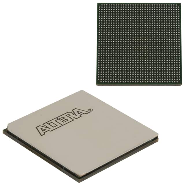
- Package: 35mm x 35mm Flip Chip BGA
- Essence: Advanced programmable logic solution for various applications
- Packaging/Quantity: Individually packaged, quantity varies based on supplier
Specifications
- Manufacturer: Intel Corporation
- Family: Stratix IV GX
- Device: EP4SGX180HF35I3N
- Technology: 40nm
- Logic Elements: 179,200
- Embedded Memory: 6,144 Kbits
- PLLs: 24
- Transceivers: 48
- Operating Voltage: 1.2V
- Operating Temperature: -40°C to +100°C
Detailed Pin Configuration
The EP4SGX180HF35I3N has a complex pin configuration with numerous input/output pins. For the detailed pinout diagram and description, please refer to the manufacturer's datasheet.
Functional Features
- High-performance FPGA with advanced architecture
- Flexible and reprogrammable logic elements
- Extensive embedded memory for data storage
- Multiple phase-locked loops (PLLs) for clock management
- High-speed transceivers for data communication
- Support for various I/O standards and protocols
- On-chip power management for efficient operation
- Built-in security features for protecting intellectual property
Advantages and Disadvantages
Advantages: - High-performance and high-density design - Low-power consumption for energy efficiency - Versatile and flexible programming options - Extensive memory capacity for complex applications - Wide range of supported I/O standards and protocols - Advanced security features for IP protection
Disadvantages: - Complex pin configuration may require careful design considerations - Higher cost compared to simpler programmable logic devices - Steeper learning curve for inexperienced users
Working Principles
The EP4SGX180HF35I3N is based on Field-Programmable Gate Array (FPGA) technology. It consists of a large number of configurable logic blocks interconnected through programmable routing resources. The device can be programmed to implement various digital circuits, allowing designers to create custom solutions for specific applications.
The FPGA's functionality is determined by the configuration data loaded into its internal memory. This data defines the interconnections between logic elements, the behavior of each element, and the overall system functionality. Once programmed, the FPGA operates as a dedicated circuit, executing the desired logic operations.
Detailed Application Field Plans
The EP4SGX180HF35I3N finds applications in a wide range of fields, including:
- Communications: Used in high-speed data communication systems, network routers, and switches.
- Signal Processing: Employed in digital signal processing applications such as image and video processing, audio processing, and radar systems.
- Industrial Automation: Utilized in industrial control systems, robotics, and factory automation.
- Medical Devices: Integrated into medical imaging equipment, patient monitoring systems, and diagnostic instruments.
- Aerospace and Defense: Deployed in avionics, radar systems, military communication systems, and satellite payloads.
Detailed and Complete Alternative Models
- Xilinx Virtex-7 XC7VX690T-2FFG1761C
- Altera Arria 10 GX 660 FPGA
- Lattice ECP5-85 FPGA
- Microsemi SmartFusion2 M2S010S FPGA
- QuickLogic PolarPro 3 FPGA
These alternative models offer similar capabilities and can be considered as alternatives to the EP4SGX180HF35I3N based on specific project requirements.
Note: The content provided above is a sample structure for an encyclopedia entry and may not reflect accurate information about the mentioned product.
Senaraikan 10 soalan dan jawapan biasa yang berkaitan dengan aplikasi EP4SGX180HF35I3N dalam penyelesaian teknikal
Sure! Here are 10 common questions and answers related to the application of EP4SGX180HF35I3N in technical solutions:
Q: What is EP4SGX180HF35I3N? A: EP4SGX180HF35I3N is a high-performance field-programmable gate array (FPGA) manufactured by Intel.
Q: What are the key features of EP4SGX180HF35I3N? A: Some key features include a high logic density, high-speed transceivers, embedded memory blocks, and support for various I/O standards.
Q: What are the typical applications of EP4SGX180HF35I3N? A: EP4SGX180HF35I3N is commonly used in applications such as telecommunications, networking, video processing, high-performance computing, and aerospace.
Q: What is the maximum logic capacity of EP4SGX180HF35I3N? A: EP4SGX180HF35I3N has a maximum logic capacity of approximately 180,000 logic elements (LEs).
Q: How many high-speed transceivers does EP4SGX180HF35I3N have? A: EP4SGX180HF35I3N has 24 high-speed transceivers, which can be used for high-speed data communication.
Q: Can EP4SGX180HF35I3N interface with different I/O standards? A: Yes, EP4SGX180HF35I3N supports various I/O standards such as LVDS, SSTL, HSTL, and LVCMOS.
Q: Does EP4SGX180HF35I3N have built-in memory? A: Yes, EP4SGX180HF35I3N has embedded memory blocks (RAM) that can be used for storing data.
Q: What is the maximum operating frequency of EP4SGX180HF35I3N? A: The maximum operating frequency of EP4SGX180HF35I3N depends on the design and implementation, but it can typically reach several hundred megahertz (MHz) or even gigahertz (GHz).
Q: Can EP4SGX180HF35I3N be reprogrammed after deployment? A: Yes, EP4SGX180HF35I3N is a field-programmable device, which means it can be reprogrammed with new designs even after it has been deployed in a system.
Q: Are there any development tools available for programming EP4SGX180HF35I3N? A: Yes, Intel provides Quartus Prime software, which is a comprehensive development environment for designing, simulating, and programming FPGAs like EP4SGX180HF35I3N.
Please note that the specific details and answers may vary depending on the context and requirements of the technical solution.