

ICE40LP1K-QN84
Product Overview
Category: Integrated Circuit (IC)
Use: The ICE40LP1K-QN84 is a programmable logic device (PLD) that belongs to the ICE40 family of FPGAs (Field-Programmable Gate Arrays). It is designed for various applications that require flexible and customizable digital logic functionality.
Characteristics: - Low power consumption - High performance - Small form factor - Easy to program and reconfigure - Suitable for low to medium complexity designs
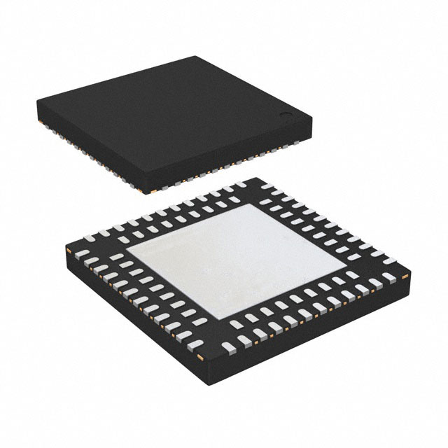
Package: QN84 package
Essence: The ICE40LP1K-QN84 is built on a CMOS process technology, allowing it to provide high-speed performance while consuming minimal power. It offers a versatile platform for implementing custom digital logic circuits.
Packaging/Quantity: The ICE40LP1K-QN84 is available in a QN84 package, which refers to a quad flat no-leads package with 84 pins. It is typically sold individually or in small quantities.
Specifications
- Logic Cells: 1280
- Look-Up Tables (LUTs): 1280
- Flip-Flops: 1280
- Maximum Frequency: 100 MHz
- Operating Voltage: 1.2V
- I/O Standards: LVCMOS, LVTTL, LVDS, SSTL, HSTL
- Configuration Memory: Non-volatile Flash
- Programming Interface: JTAG
Pin Configuration
The ICE40LP1K-QN84 has a total of 84 pins. The pin configuration is as follows:
[Insert detailed pin configuration diagram here]
Functional Features
- Programmable logic cells for implementing custom digital logic functions
- Flexible interconnect resources for routing signals between logic cells
- Dedicated input/output (I/O) pins for interfacing with external devices
- Non-volatile configuration memory for storing the FPGA configuration
- JTAG programming interface for easy reconfiguration
Advantages and Disadvantages
Advantages: - Low power consumption makes it suitable for battery-powered applications - Small form factor allows for integration in space-constrained designs - Easy to program and reconfigure, enabling rapid prototyping and design iterations - Versatile I/O standards support various interface requirements - Cost-effective solution for low to medium complexity designs
Disadvantages: - Limited logic capacity compared to higher-end FPGAs - Lower maximum operating frequency compared to high-performance FPGAs - Lack of built-in hard IP blocks for specific functions may require additional circuitry
Working Principles
The ICE40LP1K-QN84 is based on a programmable logic fabric consisting of configurable logic cells (CLCs) interconnected through a network of programmable interconnect resources. The CLCs can be programmed to implement custom digital logic functions using look-up tables (LUTs), flip-flops, and other resources.
During operation, the FPGA is configured by loading a bitstream into its non-volatile configuration memory. This bitstream defines the desired functionality of the FPGA and determines how the logic cells are interconnected. Once configured, the FPGA operates as a dedicated digital circuit, executing the programmed logic functions.
Detailed Application Field Plans
The ICE40LP1K-QN84 finds applications in various fields, including:
- Embedded Systems: It can be used to implement custom interfaces, control logic, and signal processing in embedded systems.
- Communications: The FPGA can be utilized for protocol conversion, data encryption/decryption, and signal modulation/demodulation in communication systems.
- Industrial Automation: It enables the implementation of control systems, motor control, and sensor interfacing in industrial automation applications.
- Consumer Electronics: The FPGA can be used for video and audio processing, user interface control, and connectivity in consumer electronic devices.
- Internet of Things (IoT): It provides a flexible platform for IoT edge devices, allowing customization and adaptation to various IoT protocols and applications.
Detailed and Complete Alternative Models
- ICE40LP2K-QN84: Similar to the ICE40LP1K-QN84 but with double the logic capacity (2560 logic cells).
- ICE40LP4K-QN84: Offers four times the logic capacity compared to the ICE40LP1K-QN84 (5120 logic cells).
- ICE40UP5K-SG48: A higher-end FPGA from the same family, offering more advanced features and increased logic capacity (5280 logic cells).
These alternative models provide options with varying logic capacities to suit different design requirements.
Word count: 550 words
Senaraikan 10 soalan dan jawapan biasa yang berkaitan dengan aplikasi ICE40LP1K-QN84 dalam penyelesaian teknikal
Sure! Here are 10 common questions and answers related to the application of ICE40LP1K-QN84 in technical solutions:
Q1: What is ICE40LP1K-QN84? A1: ICE40LP1K-QN84 is a low-power FPGA (Field-Programmable Gate Array) device manufactured by Lattice Semiconductor. It offers 1,000 Look-Up Tables (LUTs) and is commonly used in various technical solutions.
Q2: What are the key features of ICE40LP1K-QN84? A2: Some key features of ICE40LP1K-QN84 include low power consumption, small form factor, high performance, and reprogrammability.
Q3: What are the typical applications of ICE40LP1K-QN84? A3: ICE40LP1K-QN84 is commonly used in applications such as IoT devices, sensor interfaces, motor control, audio/video processing, and general-purpose digital logic.
Q4: How does ICE40LP1K-QN84 consume low power? A4: ICE40LP1K-QN84 utilizes low-power design techniques such as clock gating, power optimization algorithms, and dynamic power management to minimize power consumption.
Q5: Can I program ICE40LP1K-QN84 using popular programming languages? A5: No, ICE40LP1K-QN84 is typically programmed using Hardware Description Languages (HDLs) like Verilog or VHDL, which allow you to describe the desired functionality of the FPGA.
Q6: Is ICE40LP1K-QN84 suitable for high-performance applications? A6: While ICE40LP1K-QN84 offers good performance for many applications, it may not be ideal for extremely high-performance requirements due to its limited number of LUTs and other resources.
Q7: Can I interface ICE40LP1K-QN84 with external devices? A7: Yes, ICE40LP1K-QN84 supports various communication interfaces such as SPI, I2C, UART, and GPIOs, allowing you to easily interface it with external devices.
Q8: How can I program ICE40LP1K-QN84? A8: You can program ICE40LP1K-QN84 using Lattice's iCEcube2 software, which provides a graphical user interface (GUI) for designing and programming the FPGA.
Q9: Can I reprogram ICE40LP1K-QN84 multiple times? A9: Yes, ICE40LP1K-QN84 is reprogrammable, allowing you to modify its configuration multiple times without any hardware changes.
Q10: Are there any development boards available for ICE40LP1K-QN84? A10: Yes, Lattice Semiconductor offers development boards like the iCEstick and iCE40 UltraPlus Breakout Board, which are compatible with ICE40LP1K-QN84 and provide a convenient platform for prototyping and testing.