

LC4256V-3FT256BC
Product Overview
Category: Integrated Circuit (IC)
Use: The LC4256V-3FT256BC is a programmable logic device (PLD) that belongs to the family of Complex Programmable Logic Devices (CPLDs). It is designed for digital logic applications and offers high performance and flexibility.
Characteristics: - High-density programmable logic device - Low power consumption - Fast propagation delay - Flexible pin configuration - Wide operating temperature range
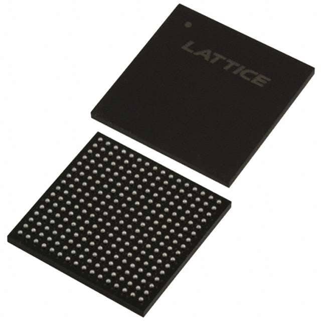
Package: The LC4256V-3FT256BC comes in a 256-ball FineLine BGA package, which provides excellent thermal and electrical performance. The package ensures reliable operation and ease of integration into various electronic systems.
Essence: The essence of the LC4256V-3FT256BC lies in its ability to implement complex digital logic functions in a single integrated circuit. It offers designers the flexibility to create custom logic solutions tailored to their specific application requirements.
Packaging/Quantity: The LC4256V-3FT256BC is typically sold in reels or trays, with a quantity of 250 units per reel/tray.
Specifications
- Logic Cells: 256
- Macrocells: 128
- Maximum Frequency: 200 MHz
- Operating Voltage: 3.3V
- I/O Pins: 156
- I/O Standards: LVTTL, LVCMOS
- JTAG Boundary Scan Support: Yes
- On-Chip Memory: 4 Kbits
- Programmable I/O Pin Placement
- Advanced Clock Management
- Built-in Security Features
Detailed Pin Configuration
The LC4256V-3FT256BC has a total of 256 pins. The pin configuration is as follows:
- Pin 1: VCCIO
- Pin 2: GND
- Pin 3: TCK
- Pin 4: TMS
- Pin 5: TDI
- Pin 6: TDO
- ...
- Pin 256: VCCIO
For a complete pin configuration diagram, please refer to the datasheet provided by the manufacturer.
Functional Features
The LC4256V-3FT256BC offers several functional features that enhance its usability and performance:
Programmability: The device can be programmed using industry-standard hardware description languages (HDLs) such as VHDL or Verilog, allowing designers to create custom logic functions.
Flexible I/O Configuration: The device supports various I/O standards, enabling seamless integration with different peripheral devices and interfaces.
Advanced Clock Management: The built-in clock management circuitry allows precise control of clock signals, facilitating synchronous operation and reducing timing issues.
On-Chip Memory: The integrated memory blocks provide additional storage for data or configuration information, enhancing the device's versatility.
Advantages and Disadvantages
Advantages: - High-density logic implementation - Low power consumption - Fast operating speed - Flexible pin configuration - Support for multiple I/O standards - Built-in security features
Disadvantages: - Limited number of logic cells compared to larger CPLDs - Higher cost compared to simpler programmable logic devices
Working Principles
The LC4256V-3FT256BC operates based on the principles of programmable logic. It consists of an array of configurable logic blocks (CLBs) interconnected through a programmable routing matrix. The CLBs contain look-up tables (LUTs), flip-flops, and other components that can be configured to implement desired logic functions.
During programming, the designer specifies the desired logic functions using a hardware description language. The programming tool then translates this description into configuration data, which is loaded into the device. Once programmed, the LC4256V-3FT256BC operates autonomously, executing the specified logic functions.
Detailed Application Field Plans
The LC4256V-3FT256BC finds applications in various fields, including:
Embedded Systems: The device can be used to implement control and interface logic in embedded systems such as industrial automation, robotics, and automotive electronics.
Communications: It can be employed in communication systems for protocol conversion, signal processing, and data routing.
Consumer Electronics: The LC4256V-3FT256BC can be utilized in consumer electronic devices like gaming consoles, set-top boxes, and smart home appliances for custom logic implementation.
Medical Devices: It can be integrated into medical equipment for controlling and monitoring functions, ensuring precise operation and reliability.
Detailed and Complete Alternative Models
- Altera MAX V CPLD: Offers similar functionality with a larger number of logic cells and I/O pins.
- Xilinx CoolRunner-II CPLD: Provides comparable features with enhanced power efficiency and lower cost.
- Lattice
Senaraikan 10 soalan dan jawapan biasa yang berkaitan dengan aplikasi LC4256V-3FT256BC dalam penyelesaian teknikal
Sure! Here are 10 common questions and answers related to the application of LC4256V-3FT256BC in technical solutions:
Q: What is LC4256V-3FT256BC? A: LC4256V-3FT256BC is a specific model of Field-Programmable Gate Array (FPGA) manufactured by Lattice Semiconductor.
Q: What are the key features of LC4256V-3FT256BC? A: Some key features of LC4256V-3FT256BC include 256 macrocells, 56 I/O pins, 3.3V operating voltage, and 256 user-configurable logic blocks.
Q: What are the typical applications of LC4256V-3FT256BC? A: LC4256V-3FT256BC is commonly used in various technical solutions such as industrial automation, telecommunications, automotive electronics, and consumer electronics.
Q: How can LC4256V-3FT256BC be programmed? A: LC4256V-3FT256BC can be programmed using Hardware Description Languages (HDLs) like VHDL or Verilog, which describe the desired functionality of the FPGA.
Q: Can LC4256V-3FT256BC be reprogrammed after initial programming? A: Yes, LC4256V-3FT256BC is a reprogrammable FPGA, allowing for flexibility in design iterations and updates.
Q: What is the power consumption of LC4256V-3FT256BC? A: The power consumption of LC4256V-3FT256BC depends on the specific design and usage scenario. It is recommended to refer to the datasheet for detailed power specifications.
Q: Does LC4256V-3FT256BC support external memory interfaces? A: Yes, LC4256V-3FT256BC supports various external memory interfaces such as SDRAM, DDR, and Flash memory.
Q: Can LC4256V-3FT256BC interface with other digital components or microcontrollers? A: Yes, LC4256V-3FT256BC can interface with other digital components or microcontrollers using standard protocols like SPI, I2C, UART, or custom communication interfaces.
Q: What development tools are available for programming LC4256V-3FT256BC? A: Lattice Semiconductor provides development tools like Lattice Diamond or Lattice Radiant software suites for designing, simulating, and programming LC4256V-3FT256BC.
Q: Are there any application-specific reference designs available for LC4256V-3FT256BC? A: Yes, Lattice Semiconductor offers application-specific reference designs and example projects that can serve as a starting point for various technical solutions using LC4256V-3FT256BC.
Please note that the answers provided here are general and may vary depending on specific requirements and use cases. It is always recommended to refer to the official documentation and datasheets for accurate and up-to-date information.