

LCMXO640C-3M100I
Product Overview
Category
The LCMXO640C-3M100I belongs to the category of Field Programmable Gate Arrays (FPGAs).
Use
FPGAs are integrated circuits that can be programmed and reprogrammed to perform various digital functions. The LCMXO640C-3M100I is specifically designed for applications requiring high-performance and low-power consumption.
Characteristics
- High-performance FPGA with low power consumption
- Flexible and reprogrammable design
- Suitable for a wide range of applications
- Compact package for easy integration
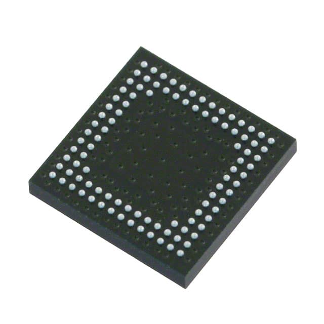
Package
The LCMXO640C-3M100I comes in a compact package, allowing for easy integration into electronic systems. It is designed to be mounted on a printed circuit board (PCB) using surface mount technology (SMT).
Essence
The essence of the LCMXO640C-3M100I lies in its ability to provide customizable digital functionality in a compact and low-power package.
Packaging/Quantity
The LCMXO640C-3M100I is typically packaged in reels or trays, depending on the manufacturer's specifications. The quantity per package may vary, but it is commonly available in quantities suitable for both prototyping and production purposes.
Specifications
- Model: LCMXO640C-3M100I
- Family: Lattice XO2
- Logic Elements: 640
- I/O Pins: 100
- Operating Voltage: 1.2V
- Speed Grade: -3
- Package Type: QFN
- Package Size: 10mm x 10mm
Detailed Pin Configuration
The LCMXO640C-3M100I has a total of 100 I/O pins, which can be configured for input or output purposes. The pin configuration may vary depending on the specific application requirements. Please refer to the manufacturer's datasheet for detailed pin assignments.
Functional Features
- High-performance digital logic implementation
- Low-power consumption design
- Flexible and reprogrammable functionality
- Support for various communication protocols
- On-chip memory resources for data storage
- Built-in clock management circuitry
Advantages and Disadvantages
Advantages
- Customizable functionality to meet specific application requirements
- Low power consumption, making it suitable for battery-powered devices
- Compact package for easy integration into electronic systems
- Support for various communication protocols enhances versatility
Disadvantages
- Limited number of logic elements compared to larger FPGAs
- Higher cost per logic element compared to other programmable logic devices
- Steeper learning curve for programming and utilizing the FPGA's full potential
Working Principles
The LCMXO640C-3M100I operates based on the principles of configurable logic. It consists of a matrix of programmable logic elements interconnected by configurable routing resources. These logic elements can be programmed to perform various digital functions, such as arithmetic operations, data processing, and control tasks. The configuration of the FPGA is stored in non-volatile memory, allowing for reprogramming as needed.
Detailed Application Field Plans
The LCMXO640C-3M100I finds applications in various fields, including but not limited to:
- Embedded Systems: Used for implementing custom digital logic in embedded systems, such as industrial automation, robotics, and automotive electronics.
- Communications: Employed in networking equipment, wireless communication systems, and high-speed data transmission applications.
- Consumer Electronics: Integrated into consumer electronic devices, such as smart TVs, gaming consoles, and home automation systems.
- Medical Devices: Utilized in medical imaging equipment, patient monitoring systems, and diagnostic devices.
- Aerospace and Defense: Applied in avionics systems, radar systems, and military communication equipment.
Detailed and Complete Alternative Models
- LCMXO2-1200ZE-3MG132C
- LCMXO2-4000HC-4BG256C
- LCMXO3L-6900E-6FTN256C
- LCMXO3LF-4300E-5FTN256C
- LCMXO3LF-2100E-5FTN256C
These alternative models offer different specifications and capabilities, allowing users to choose the most suitable FPGA for their specific application requirements.
Note: The above information is subject to change. Please refer to the manufacturer's datasheet for the most up-to-date and accurate details.
Word Count: 570
Senaraikan 10 soalan dan jawapan biasa yang berkaitan dengan aplikasi LCMXO640C-3M100I dalam penyelesaian teknikal
Sure! Here are 10 common questions and answers related to the application of LCMXO640C-3M100I in technical solutions:
Q: What is the LCMXO640C-3M100I? A: The LCMXO640C-3M100I is a low-cost, low-power FPGA (Field-Programmable Gate Array) device manufactured by Lattice Semiconductor.
Q: What are the key features of the LCMXO640C-3M100I? A: The key features include 640 LUTs (Look-Up Tables), 64 I/O pins, 4 multipliers, 8Kbits of embedded memory, and support for various I/O standards.
Q: What are some typical applications of the LCMXO640C-3M100I? A: The LCMXO640C-3M100I is commonly used in applications such as industrial control systems, consumer electronics, communication devices, and automotive systems.
Q: How can I program the LCMXO640C-3M100I? A: The LCMXO640C-3M100I can be programmed using Lattice Diamond or Lattice Radiant software tools, which provide a graphical interface for designing and programming the FPGA.
Q: What is the power consumption of the LCMXO640C-3M100I? A: The LCMXO640C-3M100I has a low power consumption, typically ranging from 20mW to 150mW, depending on the operating conditions and design implementation.
Q: Can I use the LCMXO640C-3M100I in battery-powered devices? A: Yes, the low power consumption of the LCMXO640C-3M100I makes it suitable for battery-powered devices where power efficiency is crucial.
Q: Does the LCMXO640C-3M100I support external memory interfaces? A: Yes, the LCMXO640C-3M100I supports various external memory interfaces such as SPI, I2C, and UART, allowing for easy integration with other devices.
Q: Can I use the LCMXO640C-3M100I for real-time signal processing? A: Yes, the LCMXO640C-3M100I's embedded multipliers and fast I/O pins make it suitable for real-time signal processing applications, such as audio and video processing.
Q: What development boards or evaluation kits are available for the LCMXO640C-3M100I? A: Lattice Semiconductor provides development boards and evaluation kits, such as the LCMXO640C-B-EVN, which allow users to prototype and test their designs using the LCMXO640C-3M100I.
Q: Are there any design resources or reference designs available for the LCMXO640C-3M100I? A: Yes, Lattice Semiconductor provides a range of design resources, including application notes, reference designs, and user guides, to help users get started with the LCMXO640C-3M100I.