

LFE2M70SE-6F1152I
Product Overview
Category
The LFE2M70SE-6F1152I belongs to the category of Field Programmable Gate Arrays (FPGAs).
Use
This FPGA is primarily used in electronic circuits for digital logic implementation, prototyping, and system integration.
Characteristics
- High-performance programmable logic device
- Offers flexibility and reconfigurability
- Provides a wide range of logic gates, flip-flops, and memory blocks
- Can be customized to meet specific application requirements
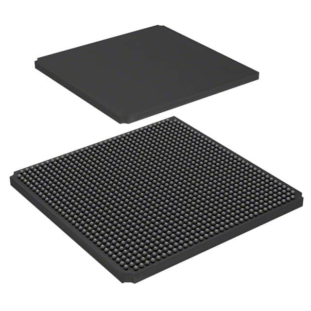
Package
The LFE2M70SE-6F1152I comes in a compact and durable package, ensuring easy handling and protection during transportation and installation.
Essence
The essence of this FPGA lies in its ability to provide a versatile platform for implementing complex digital circuits with high performance and flexibility.
Packaging/Quantity
Each package contains one LFE2M70SE-6F1152I FPGA.
Specifications
- Model: LFE2M70SE-6F1152I
- Logic Elements: 70,000
- Speed Grade: 6
- I/O Pins: 1,152
- Operating Voltage: 1.2V
- Package Type: FineLine BGA
- Temperature Range: -40°C to +100°C
Detailed Pin Configuration
The LFE2M70SE-6F1152I FPGA has a total of 1,152 I/O pins, which are organized into various banks and groups. The pin configuration details can be found in the product datasheet provided by the manufacturer.
Functional Features
- High-speed data processing capabilities
- Support for various communication protocols
- On-chip memory resources for efficient data storage
- Configurable I/O standards for interfacing with external devices
- Built-in security features for protecting sensitive information
Advantages and Disadvantages
Advantages
- Flexibility to adapt to changing design requirements
- Faster time-to-market compared to custom ASIC designs
- Lower development costs compared to traditional hardware implementations
- Reconfigurability allows for easy updates and modifications
Disadvantages
- Higher power consumption compared to dedicated hardware solutions
- Limited performance compared to application-specific integrated circuits (ASICs)
- Steeper learning curve for designers unfamiliar with FPGA programming
Working Principles
The LFE2M70SE-6F1152I FPGA operates based on the principles of configurable logic. It consists of a matrix of programmable logic elements, interconnects, and I/O blocks. The logic elements can be programmed to implement various digital functions, while the interconnects provide the necessary connections between these elements. The I/O blocks facilitate communication with external devices.
Detailed Application Field Plans
The LFE2M70SE-6F1152I FPGA finds applications in various fields, including:
- Telecommunications: Used in base stations, network routers, and switches for high-speed data processing.
- Aerospace and Defense: Employed in radar systems, avionics, and military communication equipment.
- Industrial Automation: Utilized in control systems, robotics, and machine vision applications.
- Automotive: Integrated into advanced driver-assistance systems (ADAS) and infotainment systems.
- Medical Devices: Used in medical imaging, patient monitoring, and diagnostic equipment.
Detailed and Complete Alternative Models
- LFE2M35SE-5F672C: A smaller variant with 35,000 logic elements and 672 I/O pins.
- LFE2M100SE-7FN1152C: A higher-end model with 100,000 logic elements and 1,152 I/O pins.
- LFE2M150SE-9FN1152I: A more powerful FPGA with 150,000 logic elements and 1,152 I/O pins.
These alternative models offer different combinations of logic elements, I/O pins, and performance levels to cater to diverse application requirements.
In conclusion, the LFE2M70SE-6F1152I FPGA is a high-performance programmable logic device that provides flexibility, reconfigurability, and a wide range of digital logic resources. It finds applications in various industries and offers advantages such as adaptability, faster time-to-market, and lower development costs. However, it also has limitations in terms of power consumption and performance compared to ASICs.
Senaraikan 10 soalan dan jawapan biasa yang berkaitan dengan aplikasi LFE2M70SE-6F1152I dalam penyelesaian teknikal
Sure! Here are 10 common questions and answers related to the application of LFE2M70SE-6F1152I in technical solutions:
Q: What is the LFE2M70SE-6F1152I? A: The LFE2M70SE-6F1152I is a specific model of Field-Programmable Gate Array (FPGA) manufactured by Lattice Semiconductor.
Q: What are the key features of the LFE2M70SE-6F1152I? A: Some key features of this FPGA include 70,000 Look-Up Tables (LUTs), 6-input function capability, and support for up to 1,152 I/O pins.
Q: What are the typical applications of the LFE2M70SE-6F1152I? A: This FPGA is commonly used in various technical solutions such as industrial automation, telecommunications, automotive electronics, and medical devices.
Q: How can I program the LFE2M70SE-6F1152I? A: You can program this FPGA using industry-standard Hardware Description Languages (HDLs) like VHDL or Verilog, and then use appropriate programming tools provided by Lattice Semiconductor.
Q: Can I reprogram the LFE2M70SE-6F1152I after it has been programmed once? A: Yes, FPGAs are designed to be reprogrammable, allowing you to modify the functionality of the device as needed.
Q: What is the power supply requirement for the LFE2M70SE-6F1152I? A: The LFE2M70SE-6F1152I typically requires a power supply voltage of 1.2V for its core and 3.3V for its I/O pins.
Q: Does the LFE2M70SE-6F1152I support high-speed serial communication protocols? A: Yes, this FPGA supports various high-speed serial communication protocols such as PCIe, Ethernet, USB, and SATA.
Q: Can I interface the LFE2M70SE-6F1152I with external memory devices? A: Yes, this FPGA has dedicated memory interfaces that allow you to connect external memory devices like DDR3 or DDR4 SDRAM.
Q: What development tools are available for designing with the LFE2M70SE-6F1152I? A: Lattice Semiconductor provides a suite of design tools, including Lattice Diamond software, which allows you to design, simulate, and program the FPGA.
Q: Are there any evaluation boards or reference designs available for the LFE2M70SE-6F1152I? A: Yes, Lattice Semiconductor offers evaluation boards and reference designs that can help you get started with the LFE2M70SE-6F1152I and accelerate your development process.
Please note that the specific details and answers may vary depending on the manufacturer's documentation and specifications.