

LFE3-35EA-6FN672I
Product Overview
Category: Field Programmable Gate Array (FPGA)
Use: The LFE3-35EA-6FN672I is a high-performance FPGA designed for various digital applications. It offers flexible programmability and can be configured to perform specific tasks.
Characteristics: - High-speed processing capabilities - Large number of logic elements - Low power consumption - Versatile I/O options - Robust design for reliability
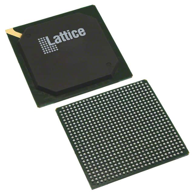
Package: The LFE3-35EA-6FN672I comes in a compact and durable package, ensuring easy handling and protection during transportation and installation.
Essence: This FPGA is an essential component in electronic systems that require customizable and reconfigurable logic functions. It enables designers to implement complex digital circuits efficiently.
Packaging/Quantity: The LFE3-35EA-6FN672I is typically sold individually or in small quantities, depending on the requirements of the customer or project.
Specifications
- Logic Elements: 35,000
- Embedded Memory: 1,080 Kbits
- Maximum User I/Os: 672
- Clock Management Tiles: 8
- DSP Blocks: 126
- Maximum Internal Frequency: 500 MHz
- Operating Voltage: 1.2V
- Package Type: FineLine BGA
- Temperature Range: -40°C to +100°C
Detailed Pin Configuration
The LFE3-35EA-6FN672I has a comprehensive pin configuration, allowing for versatile connectivity and integration within electronic systems. For a detailed pinout diagram and description, please refer to the product datasheet provided by the manufacturer.
Functional Features
- High-speed data processing: The FPGA offers fast processing capabilities, making it suitable for applications requiring real-time data handling.
- Reconfigurability: The LFE3-35EA-6FN672I can be reprogrammed to adapt to changing requirements, allowing for flexibility in system design.
- Versatile I/O options: With a large number of user I/Os, the FPGA can interface with various external devices and subsystems.
- Clock management: The integrated clock management tiles enable precise timing control and synchronization within the system.
- DSP capabilities: The FPGA includes dedicated digital signal processing blocks, enhancing its performance in applications requiring complex mathematical operations.
Advantages and Disadvantages
Advantages: - High-performance processing capabilities - Flexibility and reconfigurability - Versatile I/O options - Low power consumption - Robust design for reliability
Disadvantages: - Steep learning curve for beginners due to complexity - Higher cost compared to simpler programmable logic devices
Working Principles
The LFE3-35EA-6FN672I operates based on the principles of field-programmable gate arrays. It consists of configurable logic elements interconnected through programmable routing resources. These logic elements can be programmed to implement desired digital functions, enabling the FPGA to perform specific tasks as required by the application.
Detailed Application Field Plans
The LFE3-35EA-6FN672I finds applications in various fields, including but not limited to: - Communications systems - Industrial automation - Aerospace and defense - Medical equipment - Automotive electronics - Consumer electronics
Its versatility and high-performance characteristics make it suitable for applications that require customizable and efficient digital circuitry.
Detailed and Complete Alternative Models
- LFE3-17EA-6FN672C: A lower-cost alternative with reduced logic elements and I/O options.
- LFE3-70EA-8FN484I: A higher-end model with increased logic elements and DSP capabilities.
- LFE5UM-85F-8MG756C: A more advanced FPGA with higher capacity and enhanced features.
These alternative models offer varying specifications and capabilities, allowing designers to choose the most suitable FPGA for their specific requirements.
Note: The above information is based on the available data at the time of writing. For the most accurate and up-to-date information, please refer to the product datasheet provided by the manufacturer.
Senaraikan 10 soalan dan jawapan biasa yang berkaitan dengan aplikasi LFE3-35EA-6FN672I dalam penyelesaian teknikal
Sure! Here are 10 common questions and answers related to the application of LFE3-35EA-6FN672I in technical solutions:
Q: What is the LFE3-35EA-6FN672I? A: The LFE3-35EA-6FN672I is a field-programmable gate array (FPGA) manufactured by Lattice Semiconductor.
Q: What are the key features of the LFE3-35EA-6FN672I? A: The key features include 35,000 Look-Up Tables (LUTs), 672 pins, 6-input function capability, and low power consumption.
Q: What are some typical applications of the LFE3-35EA-6FN672I? A: The LFE3-35EA-6FN672I is commonly used in applications such as industrial automation, telecommunications, automotive systems, and medical devices.
Q: How can I program the LFE3-35EA-6FN672I? A: The LFE3-35EA-6FN672I can be programmed using various design tools provided by Lattice Semiconductor, such as Lattice Diamond or Lattice Radiant.
Q: Can the LFE3-35EA-6FN672I interface with other components or devices? A: Yes, the LFE3-35EA-6FN672I supports various communication protocols like SPI, I2C, UART, and Ethernet, allowing it to interface with other components or devices.
Q: What is the maximum operating frequency of the LFE3-35EA-6FN672I? A: The maximum operating frequency of the LFE3-35EA-6FN672I depends on the specific design and implementation, but it can typically reach frequencies of several hundred megahertz.
Q: Can the LFE3-35EA-6FN672I handle high-speed data processing? A: Yes, the LFE3-35EA-6FN672I is capable of handling high-speed data processing due to its advanced architecture and high-performance capabilities.
Q: Does the LFE3-35EA-6FN672I support security features? A: Yes, the LFE3-35EA-6FN672I offers security features such as bitstream encryption and tamper detection, ensuring the protection of sensitive information.
Q: What are the power requirements for the LFE3-35EA-6FN672I? A: The LFE3-35EA-6FN672I operates at a voltage range of 1.2V to 1.5V and requires a stable power supply with appropriate current capabilities.
Q: Where can I find additional technical documentation and support for the LFE3-35EA-6FN672I? A: You can find additional technical documentation, datasheets, application notes, and support resources on the official website of Lattice Semiconductor or by contacting their customer support team.