

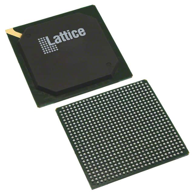
LFE3-95EA-6FN672I
Product Overview
Category
The LFE3-95EA-6FN672I belongs to the category of Field Programmable Gate Arrays (FPGAs).
Use
This FPGA is designed for various applications in the field of digital logic circuits. It provides a flexible and reconfigurable platform for implementing complex digital designs.
Characteristics
- High-performance FPGA with advanced features
- Large number of logic elements and programmable interconnects
- Low power consumption
- High-speed data processing capabilities
- Support for various communication protocols
- Configurable I/O standards
- On-chip memory resources
Package
The LFE3-95EA-6FN672I comes in a compact and durable package, ensuring easy handling and protection during transportation and installation.
Essence
The essence of this FPGA lies in its ability to provide a customizable hardware platform that can be programmed to perform specific tasks according to the user's requirements.
Packaging/Quantity
Each package contains one unit of LFE3-95EA-6FN672I FPGA.
Specifications
- Logic Elements: 95,000
- Embedded Memory: 4,608 Kbits
- Maximum User I/Os: 622
- Clock Management Tiles: 8
- DSP Blocks: 192
- Maximum Internal User Flash Memory: 2,048 Kbits
- Operating Voltage: 1.2V
- Operating Temperature Range: -40°C to 100°C
Detailed Pin Configuration
The LFE3-95EA-6FN672I has a total of 672 pins, each serving a specific purpose in the FPGA's functionality. The detailed pin configuration can be found in the product datasheet.
Functional Features
- High-speed data processing capabilities enable efficient execution of complex algorithms.
- Configurable I/O standards allow seamless integration with various external devices.
- On-chip memory resources provide storage for intermediate data and configuration settings.
- Support for various communication protocols facilitates easy interfacing with other digital systems.
- Clock management tiles enable precise timing control for synchronous operations.
- DSP blocks offer dedicated hardware for efficient implementation of arithmetic operations.
Advantages
- Flexibility: The FPGA's reconfigurable nature allows for quick prototyping and adaptation to changing requirements.
- Performance: The high logic element count and advanced features enable the FPGA to handle complex tasks efficiently.
- Power Efficiency: The low power consumption of the LFE3-95EA-6FN672I makes it suitable for battery-powered applications.
- Scalability: The FPGA can be easily scaled up or down depending on the project's needs.
- Versatility: The support for various communication protocols and configurable I/O standards enhances compatibility with different systems.
Disadvantages
- Complexity: Utilizing the full potential of an FPGA requires expertise in digital design and programming.
- Cost: FPGAs can be relatively expensive compared to other integrated circuits.
- Time-consuming Development: Designing and implementing FPGA-based solutions may require more time compared to using pre-designed ASICs.
Working Principles
The LFE3-95EA-6FN672I operates based on the principles of reconfigurable computing. It consists of a matrix of programmable logic elements interconnected through configurable routing resources. These logic elements can be programmed to perform specific functions, allowing the FPGA to execute complex digital designs.
Detailed Application Field Plans
The LFE3-95EA-6FN672I finds applications in various fields, including:
- Communications: Used in wireless base stations, network routers, and switches for high-speed data processing and protocol handling.
- Industrial Automation: Employed in control systems, robotics, and machine vision applications for real-time data processing and control.
- Aerospace and Defense: Utilized in radar systems, avionics, and military communication equipment for high-performance signal processing and encryption.
- Medical Devices: Integrated into medical imaging systems, patient monitoring devices, and laboratory equipment for data acquisition and processing.
- Automotive: Used in advanced driver assistance systems (ADAS), infotainment systems, and engine control units (ECUs) for efficient data processing and control.
Detailed and Complete Alternative Models
- LFE3-35EA-6FN672I: A smaller variant with 35,000 logic elements, suitable for less complex applications.
- LFE3-200EA-7FN672I: A higher-end model with 200,000 logic elements, offering increased performance and capacity for demanding applications.
- LFE3-12EA-8FN672I: A low-power variant with 12,000 logic elements, ideal for battery-powered portable devices.
These alternative models provide a range of options to suit different project requirements.
Word count: 600 words
Senaraikan 10 soalan dan jawapan biasa yang berkaitan dengan aplikasi LFE3-95EA-6FN672I dalam penyelesaian teknikal
Sure! Here are 10 common questions and answers related to the application of LFE3-95EA-6FN672I in technical solutions:
Q: What is the LFE3-95EA-6FN672I? A: The LFE3-95EA-6FN672I is a field-programmable gate array (FPGA) manufactured by Lattice Semiconductor.
Q: What are the key features of the LFE3-95EA-6FN672I? A: The key features include 95,000 logic cells, high-speed I/O interfaces, embedded memory blocks, and low power consumption.
Q: How can the LFE3-95EA-6FN672I be used in technical solutions? A: It can be used for various applications such as digital signal processing, image and video processing, communication systems, and industrial automation.
Q: What programming languages are supported by the LFE3-95EA-6FN672I? A: The LFE3-95EA-6FN672I supports popular hardware description languages like VHDL and Verilog.
Q: Can the LFE3-95EA-6FN672I interface with other components or devices? A: Yes, it has multiple I/O standards and interfaces, including LVDS, DDR3, PCIe, Ethernet, and more, allowing easy integration with other components.
Q: What are the power requirements for the LFE3-95EA-6FN672I? A: The power supply voltage ranges from 1.0V to 1.2V, and it has low power consumption capabilities.
Q: Is the LFE3-95EA-6FN672I suitable for high-performance applications? A: Yes, it is designed to handle high-performance requirements with its large logic capacity and high-speed interfaces.
Q: Can the LFE3-95EA-6FN672I be reprogrammed after deployment? A: Yes, it is a field-programmable device, allowing for reprogramming and updates even after deployment.
Q: Are there any development tools available for programming the LFE3-95EA-6FN672I? A: Yes, Lattice Semiconductor provides development tools like Lattice Diamond and Lattice Radiant, which support design, simulation, and programming of the FPGA.
Q: Where can I find more information about the LFE3-95EA-6FN672I? A: You can visit the official website of Lattice Semiconductor or refer to the datasheet and technical documentation provided by the manufacturer for detailed information.
Please note that the specific details and answers may vary depending on the actual product specifications and documentation.