

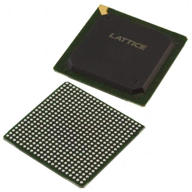
LFEC6E-3F484C
Product Overview
Category
LFEC6E-3F484C belongs to the category of Field Programmable Gate Arrays (FPGAs).
Use
This product is primarily used in digital circuit design and implementation. FPGAs provide a flexible and customizable solution for various applications, including telecommunications, automotive, aerospace, and consumer electronics.
Characteristics
- High level of integration
- Reconfigurable architecture
- Low power consumption
- Fast processing speed
- Large number of input/output pins
- Support for complex logic functions
Package
LFEC6E-3F484C is available in a compact package that ensures easy installation and compatibility with standard PCB designs.
Essence
The essence of LFEC6E-3F484C lies in its ability to provide a versatile platform for implementing complex digital circuits. Its reconfigurable nature allows designers to modify the functionality of the FPGA even after it has been manufactured.
Packaging/Quantity
LFEC6E-3F484C is typically packaged individually and is available in various quantities depending on the requirements of the user or project.
Specifications
- Logic Elements: 6,080
- Flip-Flops: 12,160
- Block RAM: 360 Kbits
- Maximum Frequency: 400 MHz
- Number of I/O Pins: 484
- Operating Voltage: 1.2V
Detailed Pin Configuration
The pin configuration of LFEC6E-3F484C is as follows:
- Pin 1: VCCIO
- Pin 2: GND
- Pin 3: IOB33
- Pin 4: IOB34
- ...
- Pin 483: IOB482
- Pin 484: IOB483
Functional Features
- High-speed data processing
- Support for various communication protocols
- On-chip memory resources
- Flexible I/O configurations
- Built-in clock management resources
- Support for partial reconfiguration
Advantages and Disadvantages
Advantages
- Flexibility in design and implementation
- Faster time-to-market compared to custom ASICs
- Lower development costs
- Reconfigurability allows for easy updates and modifications
- High level of integration reduces board space requirements
Disadvantages
- Higher power consumption compared to dedicated hardware solutions
- Limited performance compared to application-specific designs
- Steeper learning curve for designers unfamiliar with FPGA programming
Working Principles
LFEC6E-3F484C operates based on the principles of digital logic. It consists of configurable logic blocks (CLBs), interconnect resources, and input/output blocks (IOBs). The CLBs contain look-up tables (LUTs) that can be programmed to implement desired logic functions. The interconnect resources provide routing paths between different CLBs and IOBs, enabling data flow within the FPGA.
Detailed Application Field Plans
LFEC6E-3F484C finds applications in various fields, including:
- Telecommunications: Used in base stations, routers, and network switches for high-speed data processing and protocol handling.
- Automotive: Employed in advanced driver-assistance systems (ADAS) for image processing, sensor fusion, and control algorithms.
- Aerospace: Utilized in satellite communication systems, radar signal processing, and flight control systems.
- Consumer Electronics: Integrated into smart TVs, gaming consoles, and multimedia devices for video and audio processing.
Detailed and Complete Alternative Models
Some alternative models to LFEC6E-3F484C include:
- Xilinx XC7A35T-1CPG236C
- Intel Cyclone V GX EP5CGXFC7C6F23I7N
- Lattice iCE40UP5K-SG48I
- Microsemi IGLOO2 M2GL090-FG484
These models offer similar functionality and can be considered as alternatives based on specific project requirements.
In conclusion, LFEC6E-3F484C is a versatile FPGA that provides a flexible and customizable solution for digital circuit design. Its high level of integration, reconfigurable architecture, and fast processing speed make it suitable for various applications across different industries. While it has advantages such as flexibility and lower development costs, it also has disadvantages like higher power consumption and limited performance compared to dedicated hardware solutions. Nonetheless, LFEC6E-3F484C remains a valuable tool for designers seeking efficient and adaptable digital circuit implementation.
Senaraikan 10 soalan dan jawapan biasa yang berkaitan dengan aplikasi LFEC6E-3F484C dalam penyelesaian teknikal
Sure! Here are 10 common questions and answers related to the application of LFEC6E-3F484C in technical solutions:
Q: What is LFEC6E-3F484C? A: LFEC6E-3F484C is a specific model of Field-Programmable Gate Array (FPGA) manufactured by Lattice Semiconductor.
Q: What are the key features of LFEC6E-3F484C? A: LFEC6E-3F484C offers low power consumption, high performance, and high-speed connectivity options, making it suitable for various technical solutions.
Q: In which technical applications can LFEC6E-3F484C be used? A: LFEC6E-3F484C can be used in a wide range of applications such as telecommunications, industrial automation, automotive electronics, medical devices, and more.
Q: How does LFEC6E-3F484C contribute to power efficiency in technical solutions? A: LFEC6E-3F484C utilizes advanced power management techniques, allowing it to operate at lower power levels compared to traditional FPGA solutions.
Q: Can LFEC6E-3F484C support high-speed data transfer? A: Yes, LFEC6E-3F484C supports high-speed serial interfaces like PCIe, Ethernet, USB, and others, enabling fast data transfer in technical solutions.
Q: Is LFEC6E-3F484C suitable for real-time signal processing applications? A: Absolutely, LFEC6E-3F484C offers high-performance DSP blocks and dedicated resources for efficient real-time signal processing tasks.
Q: Can LFEC6E-3F484C be reprogrammed after deployment? A: Yes, LFEC6E-3F484C is a field-programmable device, meaning it can be reprogrammed even after being deployed in a technical solution.
Q: What development tools are available for programming LFEC6E-3F484C? A: Lattice Semiconductor provides various development tools like Lattice Diamond, Lattice Radiant, and Lattice Propel for programming and debugging LFEC6E-3F484C.
Q: Are there any specific design considerations when using LFEC6E-3F484C? A: Design considerations include power supply requirements, thermal management, signal integrity, and proper utilization of the FPGA's resources.
Q: Where can I find additional resources and support for LFEC6E-3F484C? A: Lattice Semiconductor's website offers comprehensive documentation, application notes, reference designs, and technical support for LFEC6E-3F484C.